Philips Semiconductors
Product specification
2 x 22 W BTL stereo car radio power
amplifier with loudspeaker protection
TDA1553Q
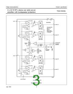
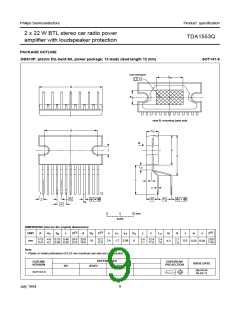
PINNING
1
2
3
4
5
6
7
IP1
input 1
8
9
GND2
OUT2B output 2B
V positive supply voltage 2
P2
power ground 2 (substrate)
GND
ground (signal)
positive supply voltage 1
V
10
P1
OUT1A output 1A
11 M/SS
12 LSP
13 IP2
mute/stand-by switch
loudspeaker protection
input 2
GND1
power ground 1 (substrate)
OUT1B output 1B
OUT2A output 2A
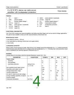
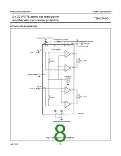
FUNCTIONAL DESCRIPTION
The TDA1553Q contains two identical amplifiers with differential input stages and can be used for bridge applications.
The gain of each amplifier is fixed at 26 dB. Special features of this device are:
Mute/stand-by switch
• low stand-by current (< 100 µA)
• low mute/stand-by switching current (low cost supply switch)
• mute facility.
Loudspeaker protection
When a short-circuit to ground is made, which forces a DC voltage across the loudspeaker of ≥ 1 V, a built-in protection
circuit becomes active and limits the DC voltage across the loudspeaker to ≤ 1 V. The delay time of the protection circuit
can be controlled by an external capacitor connected to pin 12.
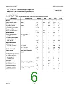
RATINGS
Limiting values in accordance with the Absolute Maximum System (IEC 134)
PARAMETER
Supply voltage
CONDITIONS
SYMBOL
MIN.
MAX.
UNIT
operating
V
V
−
−
18
V
V
P
non-operating
load dump protected
30
P
during 50 ms;
t ≥ 2.5 ms
V
−
−
−
45
6
V
r
P
Non-repetitive peak output current
Repetitive peak output current
Storage temperature range
Junction temperature
I
I
A
OSM
ORM
4
A
T
T
−55
−
+ 150
150
18
200
6
°C
°C
V
stg
j
AC and DC short-circuit-safe voltage
Energy handling capability at outputs
Reverse polarity
V
−
PSC
V = 0 V
−
mJ
V
P
V
P
−
PR
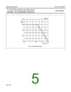
Total power dissipation
see Fig.2
−
60
W
tot
July 1994
4

 NXP [ NXP ]