Philips Semiconductors
Product specification
Remote 16-bit I/O expander for I2C-bus
PCF8575
8
LIMITING VALUES
In accordance with the Absolute Maximum Rating System (IEC 134); note 1.
SYMBOL PARAMETER
VDD
MIN.
−0.5
MAX.
UNIT
supply voltage
+6.5
±100
±100
VDD + 0.5
±20
V
IDD
ISS
VI
supply current
−
−
V
−
−
−
−
mA
mA
V
supply current
input voltage
SS − 0.5
II
DC input current
DC output current
total power dissipation
mA
mA
IO
±25
Ptot
PO
Tstg
Tamb
400
mW
mW
°C
power dissipation per output
storage temperature
100
−65
−40
+150
+85
operating ambient temperature
°C
Note
1. Stress above those listed under ‘Absolute Maximum Ratings’ may cause permanent damage to the device. This is
a stress ratings only and functional operation of the device at these or any other conditions above those indicated in
the operational sections of this specification is not implied. Exposure to absolute maximum rating conditions for
extended periods may affect device reliability.
9
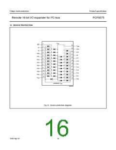
HANDLING
Inputs and outputs are protected against electrostatic discharge in normal handling. However, to be totally safe, it is
desirable to take precautions appropriate to handling MOS devices. Advice can be found in Data Handbook IC12 under
“Handling MOS Devices”.
10 CHARACTERISTICS
VDD = 2.5 to 5.5 V; VSS = 0 V; Tamb = −40 to +85 °C; unless otherwise specified.
SYMBOL
Supplies
PARAMETER
CONDITIONS
MIN.
TYP.
MAX.
UNIT
VDD
IDD
supply voltage
2.5
−
5.5
V
supply current
operating mode; no load;
−
100
200
µA
VI = VDD or VSS
;
fSCL = 400 kHz
IDD(stb)
standby current
standby mode; no load;
VI = VDD or VSS
−
2.5
10
µA
VPOR
VIL1
power-on reset voltage
note 1
−
1.2
1.8
V
V
LOW-level input voltage pins A0,
A1 and A2
0.0
−
0.2VDD
VIL2
LOW-level input voltage on all other
signal pins
0.0
−
0.3VDD
V
VIH
IL1
HIGH-level input voltage
0.7VDD
−
−
VDD
+1
V
leakage current at pins A0,
A1 and A2
VI = VDD or VSS
−1
µA
1999 Apr 07
13

 NXP [ NXP ]