PCA9557
NXP Semiconductors
8-bit I2C-bus and SMBus I/O port with reset
21. Contents
1
General description. . . . . . . . . . . . . . . . . . . . . . 1
19.3
19.4
Disclaimers . . . . . . . . . . . . . . . . . . . . . . . . . . 28
Trademarks . . . . . . . . . . . . . . . . . . . . . . . . . . 29
2
Features and benefits . . . . . . . . . . . . . . . . . . . . 1
Ordering information. . . . . . . . . . . . . . . . . . . . . 2
Ordering options. . . . . . . . . . . . . . . . . . . . . . . . 2
Block diagram . . . . . . . . . . . . . . . . . . . . . . . . . . 2
20
21
Contact information . . . . . . . . . . . . . . . . . . . . 29
Contents. . . . . . . . . . . . . . . . . . . . . . . . . . . . . . 30
3
3.1
4
5
5.1
5.2
Pinning information. . . . . . . . . . . . . . . . . . . . . . 5
Pinning . . . . . . . . . . . . . . . . . . . . . . . . . . . . . . . 5
Pin description . . . . . . . . . . . . . . . . . . . . . . . . . 5
6
System diagram. . . . . . . . . . . . . . . . . . . . . . . . . 6
7
7.1
7.2
7.3
7.3.1
7.3.2
7.3.3
7.3.4
7.4
Functional description . . . . . . . . . . . . . . . . . . . 7
Device address. . . . . . . . . . . . . . . . . . . . . . . . . 7
Control register. . . . . . . . . . . . . . . . . . . . . . . . . 7
Register descriptions . . . . . . . . . . . . . . . . . . . . 8
Register 0 - Input port register . . . . . . . . . . . . . 8
Register 1 - Output port register. . . . . . . . . . . . 8
Register 2 - Polarity inversion register . . . . . . . 8
Register 3 - Configuration register . . . . . . . . . . 8
Power-on reset . . . . . . . . . . . . . . . . . . . . . . . . . 9
RESET input. . . . . . . . . . . . . . . . . . . . . . . . . . . 9
7.5
8
Characteristics of the I2C-bus . . . . . . . . . . . . . 9
Bit transfer . . . . . . . . . . . . . . . . . . . . . . . . . . . . 9
START and STOP conditions . . . . . . . . . . . . . . 9
System configuration . . . . . . . . . . . . . . . . . . . 10
Acknowledge . . . . . . . . . . . . . . . . . . . . . . . . . 10
Bus transactions. . . . . . . . . . . . . . . . . . . . . . . 11
8.1
8.1.1
8.2
8.3
8.4
9
9.1
Application design-in information . . . . . . . . . 13
Minimizing IDD when the I/Os are used to
control LEDs. . . . . . . . . . . . . . . . . . . . . . . . . . 13
10
11
12
13
14
Limiting values. . . . . . . . . . . . . . . . . . . . . . . . . 14
Static characteristics. . . . . . . . . . . . . . . . . . . . 15
Dynamic characteristics . . . . . . . . . . . . . . . . . 16
Package outline . . . . . . . . . . . . . . . . . . . . . . . . 18
Handling information. . . . . . . . . . . . . . . . . . . . 21
15
Soldering of SMD packages . . . . . . . . . . . . . . 21
Introduction to soldering . . . . . . . . . . . . . . . . . 21
Wave and reflow soldering . . . . . . . . . . . . . . . 21
Wave soldering. . . . . . . . . . . . . . . . . . . . . . . . 21
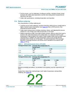
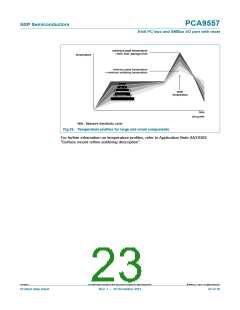
Reflow soldering. . . . . . . . . . . . . . . . . . . . . . . 22
15.1
15.2
15.3
15.4
16
17
18
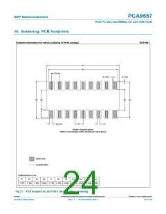
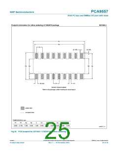
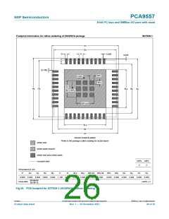
Soldering: PCB footprints. . . . . . . . . . . . . . . . 24
Abbreviations. . . . . . . . . . . . . . . . . . . . . . . . . . 27
Revision history. . . . . . . . . . . . . . . . . . . . . . . . 27
19
19.1
19.2
Legal information. . . . . . . . . . . . . . . . . . . . . . . 28
Data sheet status . . . . . . . . . . . . . . . . . . . . . . 28
Definitions. . . . . . . . . . . . . . . . . . . . . . . . . . . . 28
Please be aware that important notices concerning this document and the product(s)
described herein, have been included in section ‘Legal information’.
© NXP B.V. 2013.
All rights reserved.
For more information, please visit: http://www.nxp.com
For sales office addresses, please send an email to: salesaddresses@nxp.com
Date of release: 10 December 2013
Document identifier: PCA9557

 NXP [ NXP ]