NTAG213F/216F
NXP Semiconductors
NFC Forum T2T IC with 144/888 bytes user memory and field detection
http://www.nxp.com/index.html?m=04E141124C2880x003F31
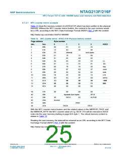
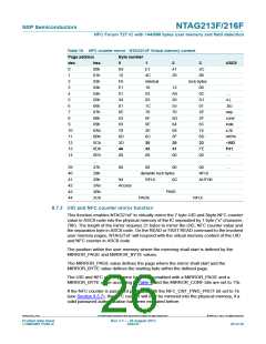
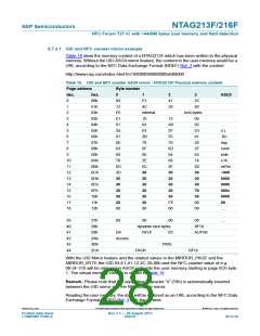
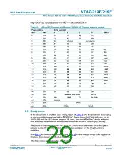
Table 19. UID and NFC counter ASCII mirror - NTAG213F Physical memory content
Page address
Byte number
dec.
0
hex.
0
1
2
3
2C
ASCII
00h
01h
02h
03h
04h
05h
06h
07h
08h
09h
0Ah
0Bh
0Ch
0Dh
0Eh
0Fh
10h
11h
12h
...
04
12
F6
E1
01
34
01
6E
63
69
78
6D
3D
31
32
38
30
33
00
E1
4C
internal
10
41
28
1
80
2
lock bytes
00
3
12
A0
2F
55
70
6D
64
68
3F
34
31
43
30
33
FE
00
4
03
0C
....
5
03
D1
4.(.
6
2B
78
01
.$U.
nxp.
com/
inde
x.ht
7
2E
8
6F
6E
2E
6C
30
2F
9
65
10
11
12
13
14
15
16
17
18
...
74
6D
ml?m
=04E
1411
24C2
880x
003F
31..
45
34
31
34
32
38
78
30
46
31
00
00
00
....
39
40
41
42
43
44
27h
28h
29h
2Ah
2Bh
2Ch
00
00
00
00
....
dynamic lock bytes
RFUI 0C
RFUI
D4
AUTH0
Access
PWD
PACK
RFUI
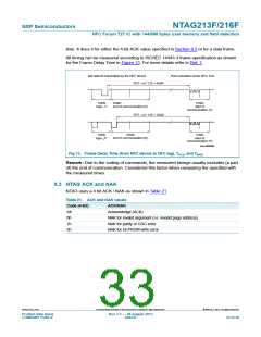
8.8 Sleep mode
If the sleep mode is enabled (see configuration bit Table 9) and the electronic device (e.g.
a microcontroller) connected to the NTAG21xF device brings the Field detection pin to
GROUND and the NFC device triggers RF reset, then the NTAG21xF device will enter
into the sleep mode where it will become invisible for the NFC device (e.g. phone).
This mode is only effective after RF reset, i.e. even if the Field detect pin is brought to
ground during HF communication, this will have no impact on the ongoing device
activities.
See Ref. 8 for additional information and Table 41 for the voltage range to be applied on
the field detection pin for effective sleep mode.
The Field detect pin shall not be left floating.
NTAG213F_216F
All information provided in this document is subject to legal disclaimers.
© NXP B.V. 2013. All rights reserved.
Product data sheet
COMPANY PUBLIC
Rev. 3.1 — 28 August 2013
262231
29 of 56

 NXP [ NXP ]