74LVC1G04
NXP Semiconductors
Single inverter
Table 9.
Measurement points
Supply voltage
VCC
Input
Output
VM
VM
1.65 V to 1.95 V
2.3 V to 2.7 V
2.7 V
0.5 VCC
0.5 VCC
1.5 V
0.5 VCC
0.5 VCC
1.5 V
3.0 V to 3.6 V
4.5 V to 5.5 V
1.5 V
1.5 V
0.5 VCC
0.5 VCC
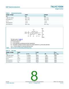
V
EXT
V
CC
R
L
V
V
O
I
G
DUT
R
T
C
L
R
L
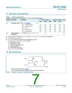
mna616
Test data is given in Table 10.
Definitions for test circuit:
RL = Load resistance.
CL = Load capacitance including jig and probe capacitance.
RT = Termination resistance should be equal to the output impedance Zo of the pulse generator.
VEXT = External voltage for measuring switching times.
Fig 9. Test circuit for measuring switching times
Table 10. Test data
Supply voltage
VCC
Input
VI
Load
CL
VEXT
tr = tf
RL
tPLH, tPHL
open
1.65 V to 1.95 V
2.3 V to 2.7 V
2.7 V
VCC
VCC
2.7 V
2.7 V
VCC
2.0 ns
2.0 ns
2.5 ns
2.5 ns
2.5 ns
30 pF
30 pF
50 pF
50 pF
50 pF
1 k
500
500
500
500
open
open
3.0 V to 3.6 V
4.5 V to 5.5 V
open
open
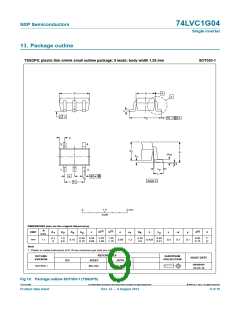
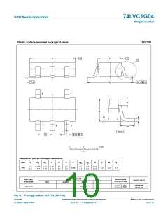
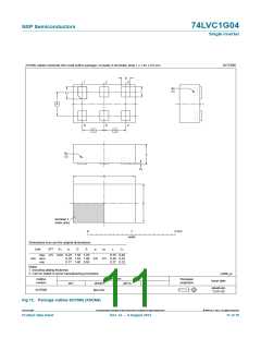
74LVC1G04
All information provided in this document is subject to legal disclaimers.
© NXP B.V. 2012. All rights reserved.
Product data sheet
Rev. 12 — 6 August 2012
8 of 19

 NXP [ NXP ]