74LVC1G04
NXP Semiconductors
Single inverter
11. Dynamic characteristics
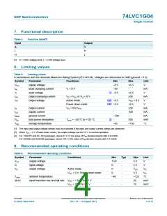
Table 8.
Dynamic characteristics
Voltages are referenced to GND (ground = 0 V). For test circuit see Figure 9.
Symbol Parameter Conditions 40 C to +85 C
40 C to +125 C Unit
Min
Typ[1]
Max
Min
Max
[2]
tpd
propagation delay A to Y; see Figure 8
VCC = 1.65 V to 1.95 V
VCC = 2.3 V to 2.7 V
1.0
0.5
0.5
0.5
0.5
-
3.0
2.0
2.3
2.0
1.6
14
7.5
5.0
5.2
4.2
3.7
-
1.0
0.5
0.5
0.5
0.5
-
9.5
6.5
7.0
5.5
5.0
-
ns
ns
ns
ns
ns
pF
VCC = 2.7 V
VCC = 3.0 V to 3.6 V
VCC = 4.5 V to 5.5 V
[3]
CPD
power dissipation VI = GND to VCC; VCC = 3.3 V
capacitance
[1] Typical values are measured at Tamb = 25 C and VCC = 1.8 V, 2.5 V, 2.7 V, 3.3 V and 5.0 V respectively.
[2] tpd is the same as tPLH and tPHL
.
[3] CPD is used to determine the dynamic power dissipation (PD in W).
PD = CPD VCC2 fi N + (CL VCC2 fo) where:
fi = input frequency in MHz;
fo = output frequency in MHz;
CL = output load capacitance in pF;
VCC = supply voltage in V;
N = number of inputs switching;
(CL VCC2 fo) = sum of outputs.
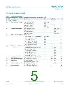
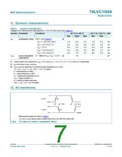
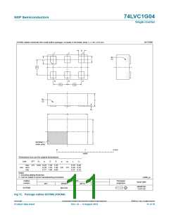
12. AC waveforms
V
I
V
A input
M
GND
t
t
PHL
PLH
V
OH
V
Y output
M
V
mna640
OL
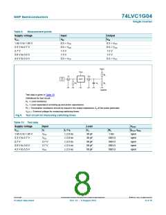
Measurement points are given in Table 9.
VOL and VOH are typical output voltage levels that occur with the output load.
Fig 8. The input A to output Y propagation delays
74LVC1G04
All information provided in this document is subject to legal disclaimers.
© NXP B.V. 2012. All rights reserved.
Product data sheet
Rev. 12 — 6 August 2012
7 of 19

 NXP [ NXP ]