74LVC1G04
NXP Semiconductors
Single inverter
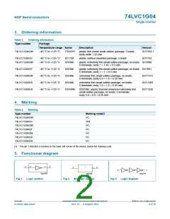
7. Functional description
Table 4.
Function table[1]
Input
Output
A
L
Y
H
L
H
[1] H = HIGH voltage level; L = LOW voltage level
8. Limiting values
Table 5.
Limiting values
In accordance with the Absolute Maximum Rating System (IEC 60134). Voltages are referenced to GND (ground = 0 V).
Symbol
VCC
IIK
Parameter
Conditions
Min
0.5
50
0.5
-
Max
+6.5
-
Unit
V
supply voltage
input clamping current
input voltage
VI < 0 V
mA
V
[1]
VI
+6.5
50
VCC + 0.5
+6.5
50
100
-
IOK
output clamping current
output voltage
VO > VCC or VO < 0 V
Active mode
mA
V
[1][2]
[1][2]
VO
0.5
0.5
-
Power-down mode
VO = 0 to VCC
V
IO
output current
mA
mA
mA
mW
C
ICC
IGND
Ptot
Tstg
supply current
-
ground current
100
-
[3]
total power dissipation
storage temperature
Tamb = 40 C to +125 C
250
+150
65
[1] The input and output voltage ratings may be exceeded if the input and output current ratings are observed.
[2] When VCC = 0 V (Power-down mode), the output voltage can be 5.5 V in normal operation.
[3] For TSSOP5 and SC-74A packages: above 87.5 C the value of Ptot derates linearly with 4.0 mW/K.
For XSON6 and X2SON5 packages: above 118 C the value of Ptot derates linearly with 7.8 mW/K.
9. Recommended operating conditions
Table 6.
Symbol
VCC
Recommended operating conditions
Parameter
Conditions
Min
Typ
Max
5.5
Unit
V
supply voltage
input voltage
output voltage
1.65
-
-
-
-
-
-
-
VI
0
5.5
V
VO
Active mode
0
VCC
5.5
VO
VO
C
VCC = 0 V; Power-down mode
0
Tamb
ambient temperature
40
+125
20
t/V
input transition rise and fall rate VCC = 1.65 V to 2.7 V
VCC = 2.7 V to 5.5 V
-
-
ns/V
ns/V
10
74LVC1G04
All information provided in this document is subject to legal disclaimers.
© NXP B.V. 2012. All rights reserved.
Product data sheet
Rev. 12 — 6 August 2012
4 of 19

 NXP [ NXP ]