74LVC1G04
NXP Semiconductors
Single inverter
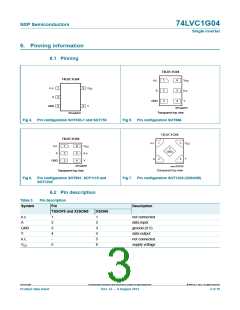
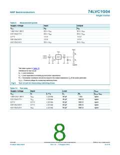
6. Pinning information
6.1 Pinning
74LVC1G04
74LVC1G04
n.c.
A
1
2
3
6
5
4
V
CC
1
2
3
5
4
n.c.
A
V
Y
CC
n.c.
Y
GND
GND
001aab619
Transparent top view
001aab618
Fig 4. Pin configuration SOT353-1 and SOT753
Fig 5. Pin configuration SOT886
74LVC1G04
74LVC1G04
n.c.
A
1
2
5
4
V
Y
CC
n.c.
A
1
2
3
6
5
4
V
CC
3
GND
n.c.
Y
GND
001aaf050
aaa-003020
Transparent top view
Transparent top view
Fig 6. Pin configuration SOT891, SOT1115 and
SOT1202
Fig 7. Pin configuration SOT1226 (X2SON5)
6.2 Pin description
Table 3.
Symbol
Pin description
Pin
Description
TSSOP5 and X2SON5
XSON6
n.c.
A
1
2
3
4
-
1
2
3
4
5
6
not connected
data input
GND
Y
ground (0 V)
data output
n.c.
VCC
not connected
supply voltage
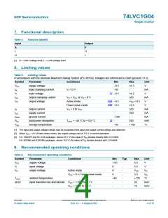
5
74LVC1G04
All information provided in this document is subject to legal disclaimers.
© NXP B.V. 2012. All rights reserved.
Product data sheet
Rev. 12 — 6 August 2012
3 of 19

 NXP [ NXP ]