74LVC1G04
NXP Semiconductors
Single inverter
3. Ordering information
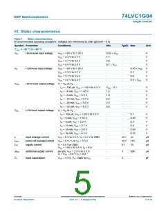
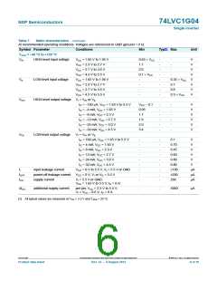
Table 1.
Ordering information
Type number
Package
Temperature range Name
Description
Version
74LVC1G04GW
40 C to +125 C
TSSOP5
plastic thin shrink small outline package; 5 leads;
body width 1.25 mm
SOT353-1
74LVC1G04GV
74LVC1G04GM
40 C to +125 C
40 C to +125 C
SC-74A
XSON6
plastic surface-mounted package; 5 leads
SOT753
plastic extremely thin small outline package; no leads; SOT886
6 terminals; body 1 1.45 0.5 mm
74LVC1G04GF
74LVC1G04GN
74LVC1G04GS
74LVC1G04GX
40 C to +125 C
40 C to +125 C
40 C to +125 C
40 C to +125 C
XSON6
XSON6
XSON6
X2SON5
plastic extremely thin small outline package; no leads; SOT891
6 terminals; body 1 1 0.5 mm
extremely thin small outline package; no leads;
6 terminals; body 0.9 1.0 0.35 mm
SOT1115
SOT1202
SOT1226
extremely thin small outline package; no leads;
6 terminals; body 1.0 1.0 0.35 mm
X2SON5: plastic thermal enhanced extremely thin
small outline package; no leads; 5 terminals;
body 0.8 0.8 0.35 mm
4. Marking
Table 2.
Marking
Type number
Marking code[1]
74LVC1G04GW
74LVC1G04GV
74LVC1G04GM
74LVC1G04GF
74LVC1G04GN
74LVC1G04GS
74LVC1G04GX
VC
V04
VC
VC
VC
VC
VC
[1] The pin 1 indicator is located on the lower left corner of the device, below the marking code.
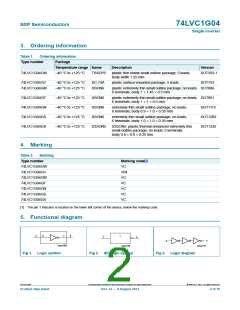
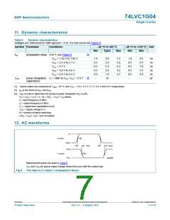
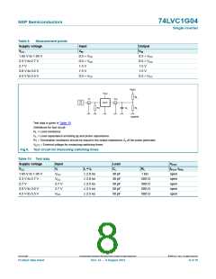
5. Functional diagram
A
Y
4
2
1
2
4
Y
A
mna108
mna109
mna110
Fig 1. Logic symbol
Fig 2. IEC logic symbol
Fig 3. Logic diagram
74LVC1G04
All information provided in this document is subject to legal disclaimers.
© NXP B.V. 2012. All rights reserved.
Product data sheet
Rev. 12 — 6 August 2012
2 of 19

 NXP [ NXP ]