Philips Semiconductors
Product specification
Dual 4-input multiplexer; 3-state
74HC/HCT253
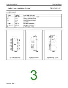
The 74HC/HCT253 have two identical 4-input multiplexers
with 3-state outputs which select two bits from four sources
selected by common data select inputs (S0, S1).
When the individual output enable (1OE, 2OE) inputs of
the 4-input multiplexers are HIGH, the outputs are forced
to the high impedance OFF-state. The “253” is the logic
implementation of a 2-pole, 4-position switch, where the
position of the switch is determined by the logic levels
applied to S0 and S1.
FEATURES
• Non-inverting data path
• 3-state outputs for bus interface
• and multiplex expansion
• Common select inputs
• Separate output enable inputs
• Output capability: bus driver
• ICC category: MSI
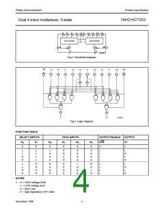
The logic equations for the outputs are:
1Y = 1OE(1l0.S1.S0+1I1.S1.S0+1I2.S1.S0+1I3.S1.S0)
2Y = 2OE(2l0.S1.S0+2I1.S1.S0+2I2.S1.S0+2I3.S1.S0)
GENERAL DESCRIPTION
The 74HC/HCT253 are high-speed Si-gate CMOS devices
and are pin compatible with low power Schottky TTL
(LSTTL). They are specified in compliance with JEDEC
standard no. 7A.
APPLICATIONS
• Data selectors
• Data multiplexers
QUICK REFERENCE DATA
GND = 0 V; Tamb = 25 °C; tr = tf = 6 ns
TYPICAL
SYMBOL
PARAMETER
CONDITIONS
UNIT
HC
HCT
tPHL/ tPLH
propagation delay
1In, 2In to nY;
Sn to nY
CL = 15 pF; VCC = 5 V
17
18
17
ns
19
3.5
55
ns
pF
pF
CI
input capacitance
3.5
55
CPD
power dissipation capacitance per multiplexer
notes 1 and 2
Notes
1. CPD is used to determine the dynamic power dissipation (PD in µW):
PD = CPD × VCC2 × fi + ∑ (CL × VCC2 × fo) where:
fi = input frequency in MHz
fo = output frequency in MHz
∑ (CL × VCC2 × fo) = sum of outputs
CL = output load capacitance in pF
VCC = supply voltage in V
2. For HC the condition is VI = GND to VCC
For HCT the condition is VI = GND to VCC − 1.5 V
ORDERING INFORMATION
See “74HC/HCT/HCU/HCMOS Logic Package Information”.
December 1990
2

 NXP [ NXP ]