Philips Semiconductors
Product specification
Octal D-type transparent latch; 3-state
74HC/HCT573
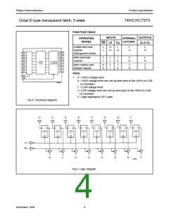
the Dn inputs enter the latches. In this
condition the latches are transparent,
i.e. a latch output will change state
each time its corresponding D-input
changes.
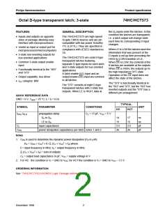
FEATURES
GENERAL DESCRIPTION
• Inputs and outputs on opposite
sides of package allowing easy
interface with microprocessors
The 74HC/HCT573 are high-speed
Si-gate CMOS devices and are pin
compatible with low power Schottky
TTL (LSTTL). They are specified in
compliance with JEDEC standard no.
7A.
• Useful as input or output port for
microprocessors/microcomputers
When LE is LOW the latches store the
information that was present at the
D-inputs a set-up time preceding the
HIGH-to-LOW transition of LE.
When OE is LOW, the contents of the
8 latches are available at the outputs.
When OE is HIGH, the outputs go to
the high impedance OFF-state.
• 3-state non-inverting outputs for
bus oriented applications
The 74HC/HCT573 are octal D-type
transparent latches featuring
separate D-type inputs for each latch
and 3-state outputs for bus oriented
applications.
A latch enable (LE) input and an
output enable (OE) input are common
to all latches.
• Common 3-state output enable
input
• Functionally identical to the “563”
and “373”
Operation of the OE input does not
affect the state of the latches.
• Output capability: bus driver
• ICC category: MSI
The “573” is functionally identical to
the “563” and “373”, but the “563” has
inverted outputs and the “373” has a
different pin arrangement.
The “573” consists of eight D-type
transparent latches with 3-state true
outputs. When LE is HIGH, data at
QUICK REFERENCE DATA
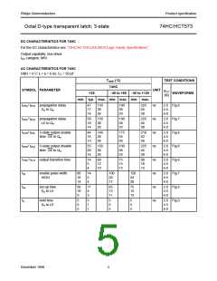
GND = 0 V; Tamb = 25 °C; tr = tf = 6 ns
TYPICAL
UNIT
SYMBOL
PARAMETER
CONDITIONS
HC
HCT
tPHL/ tPLH
propagation delay
Dn to Qn
CL = 15 pF; VCC = 5 V
14
15
3.5
26
17
15
3.5
26
ns
ns
pF
pF
LE to Qn
CI
input capacitance
CPD
power dissipation capacitance per latch notes 1 and 2
Notes
1. CPD is used to determine the dynamic power dissipation (PD in µW):
2
PD = CPD × VCC2 × fi +∑ (CL × VCC × fo) where:
fi = input frequency in MHz; fo = output frequency in MHz
∑ (CL × VCC2 × fo) = sum of outputs
CL = output load capacitance in pF; VCC = supply voltage in V
2. For HC the condition is VI = GND to VCC; for HCT the condition is VI = GND to VCC − 1.5 V
ORDERING INFORMATION
See “74HC/HCT/HCU/HCMOS Logic Package Information”.
December 1990
2

 NXP [ NXP ]