Philips Semiconductors
Product specification
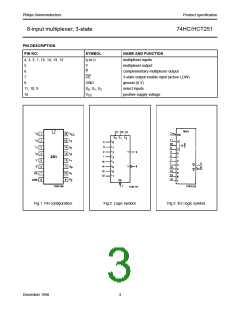
8-input multiplexer; 3-state
74HC/HCT251
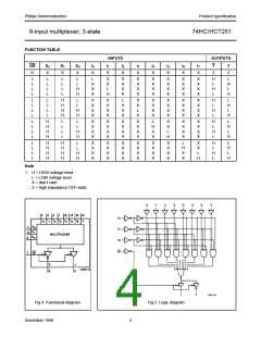
The 74HC/HCT251 are the logic implementations of
single-pole 8-position switches with the state of three
select inputs (S0, S1, S2) controlling the switch positions.
Assertion (Y) and negation (Y) outputs are both provided.
The output enable input (OE) is active LOW. The logic
function provided at the output, when activated, is:
FEATURES
• True and complement outputs
• Both outputs are 3-state for further multiplexer
expansion
• Multifunction capability
• Permits multiplexing from n-lines to one line
• Output capability: standard
• ICC category: MSI
Y = OE.(I0.S0.S1.S2 + I1.S0.S1.S2 +
+ I2.S0.S1.S2 + I3.S0.S1.S2 +
+ I4.S0.S1.S2 + I5.S0.S1.S2 +
+ I6.S0.S1.S2 + I7.S0.S1.S2)
Both outputs are in the high impedance OFF-state (Z)
when the output enable input is HIGH, allowing multiplexer
expansion by tying the outputs.
GENERAL DESCRIPTION
The 74HC/HCT251 are high-speed Si-gate CMOS devices
and are pin compatible with low power Schottky TTL
(LSTTL). They are specified in compliance with JEDEC
standard no. 7A.
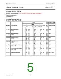
QUICK REFERENCE DATA
GND = 0 V; Tamb = 25 °C; tr = tf = 6 ns
TYPICAL
SYMBOL
PARAMETER
propagation delay
CONDITIONS
UNIT
HC
HCT
tPHL/ tPLH
CL = 15 pF; VCC = 5 V
In to Y
15
17
20
21
19
ns
In to Y
19
20
21
3.5
46
ns
ns
ns
pF
pF
Sn to Y
Sn to Y
CI
input capacitance
3.5
44
CPD
power dissipation capacitance per package
notes 1 and 2
Notes
1. CPD is used to determine the dynamic power dissipation (PD in µW):
PD = CPD × VCC2 × fi + ∑ (CL × VCC2 × fo) where:
fi = input frequency in MHz
fo = output frequency in MHz
∑ (CL × VCC2 × fo) = sum of outputs
CL = output load capacitance in pF
VCC = supply voltage in V
2. For HC the condition is VI = GND to VCC
For HCT the condition is VI = GND to VCC − 1.5 V
ORDERING INFORMATION
See “74HC/HCT/HCU/HCMOS Logic Package Information”.
December 1990
2

 NXP [ NXP ]