Philips Semiconductors
Product specification
Dual 4-input NAND gate
74HC/HCT20
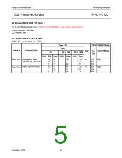
DC CHARACTERISTICS FOR 74HCT
For the DC characteristics see “74HC/HCT/HCU/HCMOS Logic Family Specifications”.
Output capability: standard
ICC category: SSI
Note to HCT types
The value of additional quiescent supply current (∆ICC) for a unit load of 1 is given in the family specifications.
To determine ∆ICC per input, multiply this value by the unit load coefficient shown in the table below.
INPUT
UNIT LOAD COEFFICIENT
nA, nB, nC, nD
0.3
AC CHARACTERISTICS FOR 74HCT
GND = 0 V; tr = tf = 6 ns; CL = 50 pF
Tamb (°C)
74HCT
TEST CONDITIONS
SYMBOL
PARAMETER
UNIT VCC WAVEFORMS
(V)
+25
−40 to +85
−40 to +125
min. typ. max. min. max. min. max.
tPHL/ tPLH propagation delay
nA, nB, nC, nD to nY
16
28
35
42
ns
ns
4.5
4.5
Fig.7
Fig.7
t
THL/ tTLH output transition time
7
15
19
22
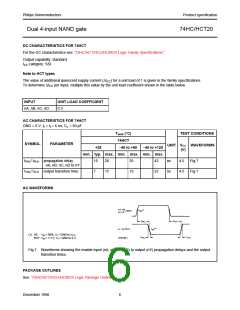
AC WAVEFORMS
(1) HC : VM = 50%; VI = GND to VCC
.
HCT: VM = 1.3 V; VI = GND to 3 V.
Fig.7 Waveforms showing the enable input (nA, nB, nC, nD) to output (nY) propagation delays and the output
transition times.
PACKAGE OUTLINES
See “74HC/HCT/HCU/HCMOS Logic Package Outlines”.
December 1990
6

 NXP [ NXP ]