Philips Semiconductors
Product specification
Dual 4-input multiplexer
74HC/HCT153
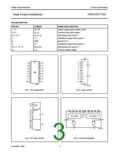
The 74HC/HCT153 have two
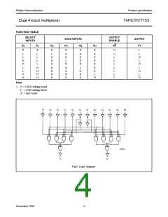
The logic equations for the outputs
are:
FEATURES
identical 4-input multiplexers which
select two bits of data from up to four
sources selected by common data
select inputs (S0, S1). The two 4-input
multiplexer circuits have individual
active LOW output enable inputs (1E,
2E) which can be used to strobe the
outputs independently. The outputs
(1Y, 2Y) are forced LOW when the
corresponding output enable inputs
are HIGH.
• Non-inverting output
1Y = 1E.(1I0.S1.S0+1I1.S1.S0+
+1I2.S1.S0+1I3.S1.S0)
• Separate enable for each output
• Common select inputs
2Y = 2E.(2I0.S1.S0+2I1.S1.S0+
+2I2.S1.S0+2I3.S1.S0)
• See ‘253” for 3-state version
• Permits multiplexing from n lines to
1 line
The “153” can be used to move data
to a common output bus from a group
of registers. The state of the select
inputs would determine the particular
register from which the data came. An
alternative application is a function
generator. The device can generate
two functions or three variables. This
is useful for implementing highly
irregular random logic.
• Enable line provided for cascading
(n lines to 1 line)
• Output capability: standard
• ICC category: MSI
The “153” is the logic implementation
of a 2-pole, 4-position switch, where
the position of the switch is
determined by the logic levels applied
to S0 and S1.
GENERAL DESCRIPTION
The 74HC/HCT153 are high-speed
Si-gate CMOS devices and are pin
compatible with low power Schottky
TTL (LSTTL). They are specified in
compliance with JEDEC standard
no. 7A.
The “153” is similar to the “253” but
has standard outputs.
QUICK REFERENCE DATA
GND = 0 V; Tamb = 25 °C; tr = tf = 6 ns
TYPICAL
UNIT
SYMBOL
PARAMETER
CONDITIONS
HC
HCT
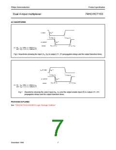
tPHL/ tPLH
propagation delay
1In, 2In to nY
Sn to nY
CL = 15 pF; VCC = 5 V
14
15
10
3.5
30
16
17
11
ns
ns
ns
pF
pF
nE to nY
CI
input capacitance
3.5
30
CPD
power dissipation capacitance per multiplexer notes 1 and 2
Notes
ORDERING INFORMATION
1. CPD is used to determine the dynamic power dissipation (PD in µW):
PD = CPD × VCC2 × fi + ∑ (CL × VCC2 × fo) where:
fi = input frequency in MHz
See “74HC/HCT/HCU/HCMOS Logic
Package Information”.
fo = output frequency in MHz
CL = output load capacitance in pF
VCC = supply voltage in V
∑ (CL × VCC2 × fo) = sum of outputs
2. For HC the condition is VI = GND to VCC
For HCT the condition is VI = GND to VCC − 1.5 V
December 1990
2

 NXP [ NXP ]