PAM8403
Filterless 3W Class-D Stereo Audio Amplifier
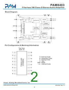
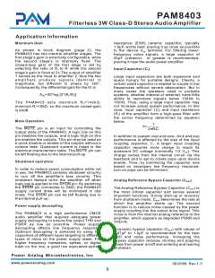
Pin Descriptions
Pin Number
Pin Name
+OUT_L
Description
1
2
Left Channel Positive Output
Power GND
PGND
-OUT_L
PVDD
3
Left Channel Negative Output
Power VDD
4
5
Mute Control Input(active low)
MUTE
VDD
INL
6
Analog VDD
7
Left Channel Input
8
VREF
NC
Internal analog reference, connect a bypass capacitor from VREF to GND
9
No connect
10
11
12
13
14
15
16
INR
Right Channel Input
Analog GND
GND
Shutdown Control Input (active low)
Power VDD
SHDN
PVDD
-OUT_R
PGND
Right Channel Negative Output
Power GND
+OUT_R
Right Channel Positive Output
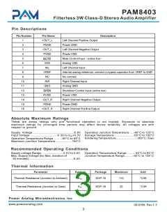
Absolute Maximum Ratings
These are stress ratings only and functional operation is not implied. Exposure to absolute
maximum ratings for prolonged time periods may affect device reliability. All voltages are with
respect to ground.
Supply Voltage............................................6.6V
Input Voltage.............................-0.3V to VDD+0.3V
Operation Temperature Range.........-40°C to 85°C
Maximum Junction Temperature..................150°C
Operation Junction Temperature.....-40°C to 125°C
Storage Temperature.....................-65°C to 150°C
Soldering Temperature.......................300°C, 5sec
Recommended Operating Conditions
Supply voltage Range........................2.5V to 5.5V
Max. Supply Voltage (for Max. duration of
30 minutes)................................................6.4V
Operation Temperature Range.........-40°C to 85°C
Junction Temperature Range.........-40°C to 125°C
Thermal Information
Parameter
Symbol
Package
Maximum
Unit
Thermal Resistance (Junction to Ambient)
θJA
SOP-16
110
°C/W
Thermal Resistance (Junction to Case)
θJC
SOP-16
23
°C/W
Power Analog Microelectronics,Inc
www.poweranalog.com
09/2008 Rev 1.3
3

 PAM [ POWER ANALOG MICOELECTRONICS ]