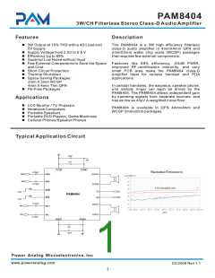
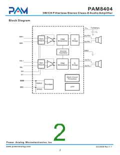
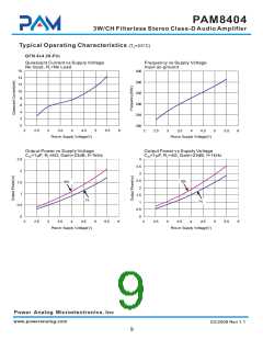
PAM8404
3W/CH Filterless Stereo Class-D Audio Amplifier
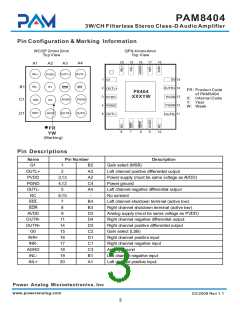
Pin Configuration & Marking Information
WCSP 2mmx2mm
Top View
QFN 4mmx4mm
Top View
20
19
18
17
16
A4
A1
A3
A2
INL+
OUTL-
OUTL+
PVDD
1
2
3
4
5
G0 15
14
G1
INL-
INR-
INR+
G1
G0
B1
C1
SDL
SDR
OUTR+
OUTL+
PVDD
PGND
OUTL-
FR: Product Code
of PAM8404
X: Internal Code
Y: Year
W: Week
P8404
XXXYW
13
PVDD
AGND
PGND
PGND 12
AVDD
OUTR-
OUTR+
D1
11
OUTR-
FR
YW
6
7
8
9
10
(Marking)
Pin Descriptions
Name
G1
Pin Number
B2
Description
1
2
Gain select (MSB)
Left channel positive differential output
OUTL+
PVDD
PGND
OUTL-
NC
A3
A2
C4
A4
-
3,13
4,12
5
Power supply (must be same voltage as AVDD)
Power ground
Left channel negative differential output
No connect
6,10
7
SDL
B4
B3
D2
D4
D3
C2
D1
C1
C3
B1
A1
Left channel shutdown terminal (active low)
Right channel shutdown terminal (active low)
Analog supply (must be same voltage as PVDD)
Right channel negative differential output
Right channel positive differential output
Gain select (LSB)
SDR
8
AVDD
OUTR-
OUTR+
G0
9
11
14
15
16
17
18
19
20
INR+
INR-
Right channel positive input
Right channel negative input
AGND
INL-
Analog ground
Left channel negative input
INL+
Left channel positive input
Power Analog Microelectronics,Inc
www.poweranalog.com
03/2009 Rev 1.1
3

 PAM [ POWER ANALOG MICOELECTRONICS ]