4.I/O Terminal
4.1.Pin Assignment
CN1,CN2
No.
1
Symbol
FLM
LP
Level
H / L
H / L
H / L
H / L
―
Function
First Line Marker
Data Latch Signal
2
CP
Clock Signal for Shifting Data
Alternate Signal for LCD Drive
Voltage Level for LCD Contrast Adjustment
Power Supply for Logic
Power Supply (0V, GND)
Power Supply for LCD Drive
Display Data
3
M
4
VADJ
VCC
VSS
5
―
6
―
7
VEE
D0
―
8
H / L
H / L
H / L
H / L
H / L
-
9
D1
Display Data
10
11
12
13
14
D2
Display Data
D3
Display Data
DISPOFF
NC
Display Control Signal H : Display on L : Display off
Non-connection
CN3
No.
1
Symbol
FL HOT
NC
Level
-
Function
Power Supply for CFL (HOT)
Non-connection
2
-
3
NC
-
Non-connection
4
FL GND
-
Power Supply for CFL (GND)
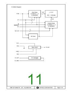
4.2.Example of Power Supply
It is recommended to apply a potentiometer for the contrast adjust due to the tolerance
of the driving voltage and its temperature dependence.
VCC
VCC (+Voltage)
R1
VR
R2
VADJ
MODULE
VEE
VSS
VEE (-Voltage)
VSS (0V)
~
R1+R2+VR=10 20K
Ω
DMF-50174ZNB-FW (AT) No.2000-0166
OPTREX CORPORATION
Page 10/18
OPTREX

 OPTREX [ OPTREX CORPORATION ]