UC3844B, UC3845B, UC2844B, UC2845B
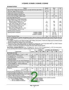
MAXIMUM RATINGS
Rating
Symbol
, V
Value
Unit
V
Bias and Driver Voltages (Zero Series Impedance, see also Total Device spec) (Note 1)
Total Power Supply and Zener Current
V
CC
36
C
(I + I )
30
mA
A
CC
Z
Output Current, Source or Sink (Note 2)
I
O
1.0
5.0
Output Energy (Capacitive Load per Cycle)
Current Sense and Voltage Feedback Inputs
Error Amp Output Sink Current
W
mJ
V
V
in
− 0.3 to + 5.5
10
I
O
mA
Power Dissipation and Thermal Characteristics
D Suffix, Plastic Package, SOIC−14 Case 751A
Maximum Power Dissipation @ T = 25°C
P
862
145
mW
°C/W
A
D
Thermal Resistance, Junction−to−Air
R
q
JA
D1 Suffix, Plastic Package, SOIC−8 Case 751
Maximum Power Dissipation @ T = 25°C
P
702
178
mW
°C/W
A
D
Thermal Resistance, Junction−to−Air
R
q
JA
N Suffix, Plastic Package, Case 626
Maximum Power Dissipation @ T = 25°C
1.25
100
W
°C/W
P
A
D
Thermal Resistance, Junction−to−Air
Operating Junction Temperature
Operating Ambient Temperature
R
q
JA
T
+150
°C
°C
J
UC3844B, UC3845B
UC2844B, UC2845B
UC3844BV, UC3845BV
T
A
0 to +70
−25 to +85
−40 to +105
Storage Temperature Range
T
stg
− 65 to +150
°C
Stresses exceeding Maximum Ratings may damage the device. Maximum Ratings are stress ratings only. Functional operation above the
Recommended Operating Conditions is not implied. Extended exposure to stresses above the Recommended Operating Conditions may affect
device reliability.
1. The voltage is clamped by a zener diode (see page 9 Under Voltage Lockout section). Therefore this voltage may be exceeded as long as
the total power supply and zener current is not exceeded.
2. Maximum package power dissipation limits must be observed.
3. This device series contains ESD protection and exceeds the following tests: Human Body Model 4000 V per JEDEC Standard
JESD22-A114B, Machine Model Method 200 V per JEDEC Standard JESD22-A115-A
4. This device contains latch-up protection and exceeds 100 mA per JEDEC Standard JESD78
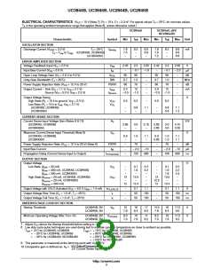
ELECTRICAL CHARACTERISTICS (V = 15 V [Note 5], R = 10 k, C = 3.3 nF. For typical values T = 25°C, for min/max values
CC
T
T
A
T is the operating ambient temperature range that applies [Note 6], unless otherwise noted.)
A
UC284xB
UC384xB, xBV, NCV384xBV
Characteristic
REFERENCE SECTION
Reference Output Voltage (I = 1.0 mA, T = 25°C)
Symbol
Min
Typ
Max
Min
Typ
Max
Unit
V
ref
4.95
−
5.0
2.0
3.0
0.2
−
5.05
20
25
−
4.9
−
5.0
2.0
3.0
0.2
−
5.1
20
V
mV
mV
mV/°C
V
O
J
Line Regulation (V = 12 V to 25 V)
Reg
CC
line
load
S
Load Regulation (I = 1.0 mA to 20 mA)
Reg
−
−
25
O
Temperature Stability
T
−
−
−
Total Output Variation over Line, Load, & Temperature
Output Noise Voltage (f = 10 Hz to 10 kHz, T = 25°C)
V
ref
4.9
−
5.1
−
4.82
−
5.18
−
V
n
50
50
mV
J
Long Term Stability (T = 125°C for 1000 Hours)
S
−
5.0
− 85
−
−
5.0
− 85
−
mV
mA
A
Output Short Circuit Current
I
− 30
−180
− 30
−180
SC
OSCILLATOR SECTION
Frequency
T = 25°C
f
49
48
52
−
55
56
49
48
52
−
55
56
kHz
J
OSC
T = T to T
A
low
high
T = 25°C (R = 6.2 k, C = 1.0 nF)
225
250
275
225
250
275
J
T
T
Frequency Change with Voltage (V = 12 V to 25 V)
Df
Df
/DV
/DT
−
−
−
0.2
1.0
1.6
1.0
−
−
−
−
0.2
0.5
1.6
1.0
−
%
%
V
CC
OSC
Frequency Change w/ Temperature (T = T to T
)
A
low
high
OSC
Oscillator Voltage Swing (Peak−to−Peak)
V
−
−
OSC
5. Adjust V above the Startup threshold before setting to 15 V.
CC
6. Low duty cycle pulse techniques are used during test to maintain junction temperature as close to ambient as possible.
T
= 0°C for UC3844B, UC3845B
= − 25°C for UC2844B, UC2845B
= − 40°C for UC384xBV, NCV384xBV
T
= + 70°C for UC3844B, UC3845B
= + 85°C for UC2844B, UC2845B
=+105°C for UC3844BV, UC3845BV
= +125°C for NCV384xBV
low
high
http://onsemi.com
2

 ONSEMI [ ONSEMI ]