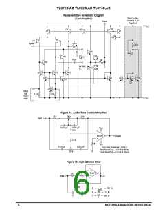
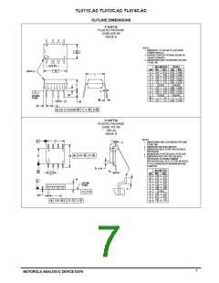
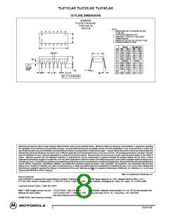
TL071C,AC TL072C,AC TL074C,AC
ELECTRICAL CHARACTERISTICS (V
CC
= 15 V, V
= –15 V, T = 25°C, unless otherwise noted.)
EE A
Characteristics
Symbol
Min
Typ
Max
Unit
Input Offset Voltage (R ≤ 10 k, V
= 0)
V
IO
mV
S
CM
TL071C, TL072C
TL074C
TL07_AC
–
–
–
3.0
3.0
3.0
10
10
6.0
Average Temperature Coefficient of Input Offset Voltage
∆V /∆T
IO
–
10
–
µV/°C
R
= 50 Ω, T = T
to T
(Note 1)
high
0) (Note 2)
S
A
low
Input Offset Current (V
TL07_C
I
IO
pA
CM =
–
–
5.0
5.0
50
50
TL07_AC
Input Bias Current (V
TL07_C
TL07_AC
= 0) (Note 2)
I
IB
pA
CM
–
–
30
30
200
200
12
10
Input Resistance
r
i
–
–
Ω
Common Mode Input Voltage Range
V
ICR
V
TL07_C
TL07_AC
±10
±11
15, –12
15, –12
–
–
Large–Signal Voltage Gain (V = ±10 V, R ≥ 2.0 k)
A
VOL
V/mV
O
L
TL07_C
TL07_AC
25
50
150
150
–
–
Output Voltage Swing (Peak–to–Peak)
(R = 10 k)
V
O
24
28
–
V
L
Common Mode Rejection Ratio (R ≤ 10 k)
TL07_C
TL07_AC
CMRR
PSRR
dB
S
70
80
100
100
–
–
Supply Voltage Rejection Ratio (R ≤ 10 k)
dB
S
TL07_C
TL07_AC
70
80
100
100
–
–
Supply Current (Each Amplifier)
Unity Gain Bandwidth
I
–
–
–
1.4
4.0
13
2.5
–
mA
MHz
v/µs
D
BW
SR
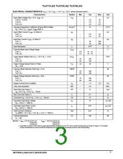
Slew Rate (See Figure 1)
–
V
= 10 V, R = 2.0 k, C = 100 pF
L L
in
Rise Time (See Figure 1)
Overshoot (V = 20 mV, R = 2.0 k, C = 100 pF)
t
–
–
–
0.1
10
18
–
–
–
µs
r
OS
%
in
Equivalent Input Noise Voltage
= 100 Ω, f = 1000 Hz
L
L
e
n
nV/√Hz
R
S
Equivalent Input Noise Current
= 100 Ω, f = 1000 Hz
i
–
–
–
0.01
0.01
120
–
–
–
pA/√Hz
n
R
S
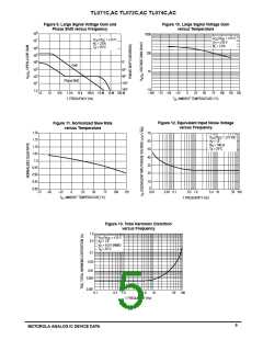
Total Harmonic Distortion
THD
CS
%
V
O
(RMS) = 10 V, R ≤ 1.0 k, R ≥ 2.0 k, f = 1000 Hz
S
L
Channel Separation
= 100
dB
A
V
NOTES: 1. T
= 0°C for TL071C,AC
0°C for TL072C,AC
0°C for TL074C,AC
T
T
T
= 70°C for TL071C,AC
= 70°C for TL072C,AC
= 70°C for TL074C,AC
low
high
high
high
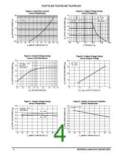
2. Input Bias currents of JFET input op amps approximately double for every 10°C rise in junction temperature as shown in Figure 3. To maintain
junction temperature as close to ambient temperature as possible, pulse techniques must be used during testing.
3
MOTOROLA ANALOG IC DEVICE DATA

 ONSEMI [ ONSEMI ]