NE5532, SA5532, SE5532, NE5532A, SE5532A
+
_
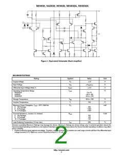
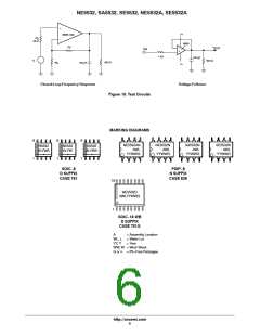
Figure 1. Equivalent Schematic (Each Amplifier)
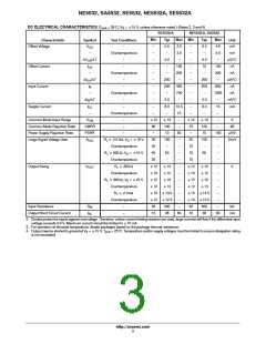
MAXIMUM RATINGS
Rating
Symbol
Value
"22
Unit
V
Supply Voltage
V
S
Input Voltage
V
IN
"V
V
SUPPLY
Differential Input Voltage (Note 1)
V
DIFF
"0.5
V
Operating Temperature Range
NE5532/A
T
amb
°C
0 to 70
−40 to +85
−55 to +125
SA5532
SE5532/A
Storage Temperature
Junction Temperature
T
−65 to +150
°C
°C
stg
T
150
j
Maximum Power Dissipation, T
= 25°C (Still-Air)
P
D
mW
amb
8
8
D8 Package
N Package
780
1200
1200
16 D Packagee
Thermal Resistance, Junction−to−Ambient
R
°C/W
°C
q
JA
8
8
D8 Package
N Package
182
130
140
16 D Packagee
Lead Soldering Temperature (10 sec max)
T
230
sld
Stresses exceeding Maximum Ratings may damage the device. Maximum Ratings are stress ratings only. Functional operation above the
RecommendedOperating Conditions is not implied. Extended exposure to stresses above the Recommended Operating Conditions may affect
device reliability.
1. Diodes protect the inputs against overvoltage. Therefore, unless current-limiting resistors are used, large currents will flow if the differential input
voltage exceeds 0.6 V. Maximum current should be limited to "10 mA.
http://onsemi.com
2

 ONSEMI [ ONSEMI ]