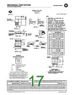
MECHANICAL CASE OUTLINE
PACKAGE DIMENSIONS
DFNW10, 3x3, 0.5P
CASE 507AG
ISSUE B
1
DATE 14 APR 2020
SCALE 2:1
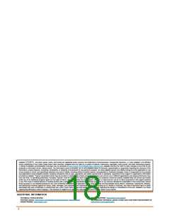
GENERIC
MARKING DIAGRAM*
1
XXXXX
XXXXX
ALYWG
G
XXXXX = Specific Device Code
A
L
= Assembly Location
= Wafer Lot
Y
W
G
= Year
= Work Week
= Pb−Free Package
(Note: Microdot may be in either location)
*This information is generic. Please refer to
device data sheet for actual part marking.
Pb−Free indicator, “G” or microdot “ G”,
may or may not be present. Some products
may not follow the Generic Marking.
Electronic versions are uncontrolled except when accessed directly from the Document Repository.
Printed versions are uncontrolled except when stamped “CONTROLLED COPY” in red.
DOCUMENT NUMBER:
DESCRIPTION:
98AON73716G
DFNW10, 3x3, 0.5P
PAGE 1 OF 1
ON Semiconductor and
are trademarks of Semiconductor Components Industries, LLC dba ON Semiconductor or its subsidiaries in the United States and/or other countries.
ON Semiconductor reserves the right to make changes without further notice to any products herein. ON Semiconductor makes no warranty, representation or guarantee regarding
the suitability of its products for any particular purpose, nor does ON Semiconductor assume any liability arising out of the application or use of any product or circuit, and specifically
disclaims any and all liability, including without limitation special, consequential or incidental damages. ON Semiconductor does not convey any license under its patent rights nor the
rights of others.
© Semiconductor Components Industries, LLC, 2018
www.onsemi.com

 ONSEMI [ ONSEMI ]