NCP562, NCP563
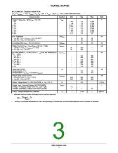
ELECTRICAL CHARACTERISTICS
(V = V
+ 1.0 V, V = V , C = 1.0 m F, C = 1.0 m F, T = 25°C, unless otherwise noted.)
enable in in out J
in
out(nom.)
Characteristic
Symbol
Min
Typ
Max
Unit
Output Voltage (TA = 25°C, I = 1.0 mA)
V
out
V
out
1.5 V
1.8 V
2.5 V
2.7 V
2.8 V
3.0 V
3.3 V
5.0 V
1.455
1.746
2.425
2.646
2.744
2.940
3.234
4.9
1.5
1.8
2.5
2.7
2.8
3.0
3.3
5.0
1.545
1.854
2.575
2.754
2.856
3.060
3.366
5.1
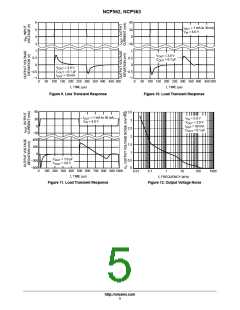
Line Regulation
Reg
mV
line
1.5 V−4.4 V (V = V
+ 1.0 V to 6.0 V
−
−
10
10
20
20
in
o(nom.)
4.5 V−5.0 V (V = 5.5 V to 6.0 V)
in
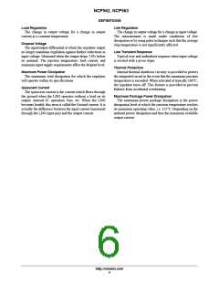
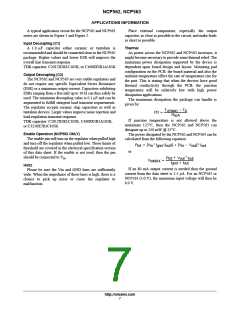
Load Regulation (I = 10 mA to 80 mA)
Reg
−
20
40
mV
mA
out
load
Output Current (V = (V at I = 80 mA) −3.0%)
I
o(nom.)
out
out
out
1.5 V to 3.9 V (V = V
+ 2.0 V)
80
80
280
280
−
−
in
out(nom.)
4.0 V−5.0 V (V = 6.0 V)
in
Dropout Voltage (T = −40°C to 85°C, I = 80 mA, Measured at
V −V
in out
mV
A
out
V
−3.0%)
out
1.5 V−1.7 V
1.8 V−2.4 V
2.5 V−2.6 V
2.7 V−2.9 V
3.0 V−3.2 V
3.3 V−4.9 V
5.0 V
−
−
−
−
−
−
−
550
400
250
230
200
190
140
800
550
400
400
350
350
250
Quiescent Current
(Enable Input = 0 V)
I
Q
m
A
−
−
0.1
2.5
1.0
6.0
(Enable Input = V , I = 1.0 mA to I
)
in out
o(nom.)
Output Short Circuit Current
I
mA
out(max)
1.5 V to 3.9 V (V = V
+ 2.0 V)
150
150
300
300
600
600
in
nom
4.0 V−5.0 V (V = 6.0 V)
in
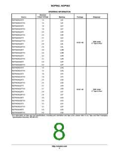
Output Voltage Noise (f = 100 Hz to 100 kHz, V = 3.0 V)
V
n
−
100
−
m
V
r
m
s
out
Enable Input Threshold Voltage (NCP562 ONLY)
(Voltage Increasing, Output Turns On, Logic High)
(Voltage Decreasing, Output Turns Off, Logic Low)
V
th(en)
V
1.3
−
−
−
−
0.3
Output Voltage Temperature Coefficient
T
C
−
"100
−
ppm/°C
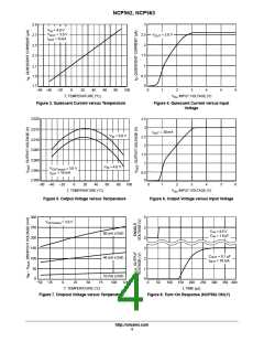
3. Maximum package power dissipation limits must be observed.
T
*T
A
qJA
J(max)
PD +
R
4. Low duty cycle pulse techniques are used during testing to maintain the junction temperature as close to ambient as possible.
http://onsemi.com
3

 ONSEMI [ ONSEMI ]