NCP5316
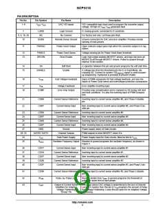
PIN DESCRIPTION
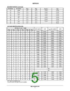
Pin No.
Pin Symbol
−V
Pin Name
Description
VID−compatible logic input used to program the converter output
1−6
V
DAC VID Inputs
ID0
ID5
voltage. All high on V −V generates fault.
ID0
ID4
7
8, 9, 19, 20
10
LGND
NC
Logic Ground
No Connect
IC analog ground; connected to IC substrate.
For factory test only. Let these pins float.
SGND
Remote Sense Ground
Ground connection for DAC and error amplifier. Provides remote
sensing of load ground.
11
PWRGD
Power Good Output
Open collector output goes high when the converter output is in reg-
ulation.
12
13
PWRLS
DRVON
Power Good Sense
Drive Enable
Voltage sensing pin for Power Good lower threshold.
Logic high output enables MOSFET drivers, and logic low turns all
MOSFETs off through MOSFET drivers. Pulled to ground through
internal 70 kW resistor.
14
15
SS
Soft Start
Enable
A capacitor between this pin and ground programs the soft start time.
A voltage less than the threshold puts the IC in Fault Mode, dis-
ENABLE
charging SS. Connect to system VID
signal to control power-
PWRGD
up sequencing. Hysteresis is provided to prevent chatter.
16
V
FFB
Fast Voltage Feedback
Input of PWM comparator for fast voltage feedback, and also the
inputs of Power Good sense and overvoltage protection comparators
17
18
V
Voltage Feedback
Error Amp Output
Error amplifier inverting input.
FB
COMP
Provides loop compensation and is clamped by SS during soft start
and fault conditions. It is also the inverting input of PWM compara-
tors.
21
22
CS6N
CS6P
Current Sense Reference
Current Sense Input
Inverting input to current sense amplifier #6, and Phase 6 disable
pin.
Non−inverting input to current sense amplifier #6, and Phase 6 dis-
able pin.
23
24
CS5N
CS5P
Current Sense Reference
Current Sense Input
Current Sense Reference
Current Sense Input
Ground
Inverting input to current sense amplifier #5.
Non−inverting input to current sense amplifier #5.
Inverting input to current sense amplifier #4.
Non−inverting input to current sense amplifier #4.
Power supply return of Gate circuits.
25
CS4N
26
CS4P
27
GND
28−33
34
GATE6−GATE1
Channel Outputs
PWM outputs to drive MOSFET driver ICs.
V
CC
Gate Power Supply
Power Supply Input for Gate circuits. Must be tied to V
.
CCL
35
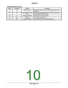
R
Oscillator Frequency Adjust Resistor to ground programs the oscillator frequency, as shown in
Figure 5.
OSC
36
37
38
39
40
CS1P
CS1N
CS2P
CS2N
CS3P
Current Sense Input
Current Sense Reference
Current Sense Input
Non−inverting input to current sense amplifier #1.
Inverting input to current sense amplifier #1.
Non−inverting input to current sense amplifier #2.
Inverting input to current sense amplifier #2.
Current Sense Reference
Current Sense Input
Non−inverting input to current sense amplifier #3, and Phase 3 dis-
able pin.
41
42
43
CS3N
Current Sense Reference
Pulse−by−Pulse Limit
Inverting input to current sense amplifier #3, and Phase 3 disable
pin.
IP
LIM
Resistor divider from V
to ground programs the threshold of
REF
pulse−by−pulse limit of each phase.
V
DRP
Output of Current Sense
Amplifiers for Adaptive
Voltage Positioning:
“Droop” Pin
The offset above DAC voltage is proportional to the sum of inductor
current. A resistor from this pin to V programs the amount of Adap-
FB
tive Voltage Positioning. Leave this pin open for no Adaptive Voltage
Positioning.
http://onsemi.com
9

 ONSEMI [ ONSEMI ]