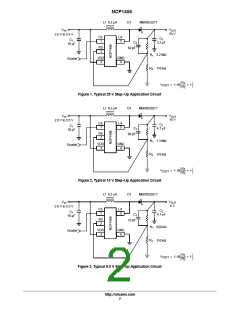
NCP1406
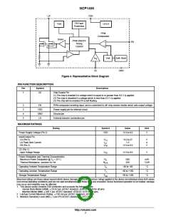
DISSIPATION RATINGS
Power Rating
Derating Factor
Power Rating
Power Rating
@T
ꢀ
255C
@T
ꢁ
255C
@T = 705C
@T =
A
855C
Package
A
A
A
TSOP−5
500 mW
4.0 mW/°C
320 mW
260 mW
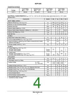
ELECTRICAL CHARACTERISTICS (V
otherwise noted.)
= 25 V, T = −40_C to +85_C for min/max values, typical values are at T = 25_C, unless
OUT
A
A
Characteristic
Symbol
Min
Typ
Max
Unit
ON/OFF TIMING CONTROL
Minimum Off Time (V = 3.0 V, V = 0 V)
t
off
0.08
0.58
84
−
0.13
0.90
90
0.20
1.40
96
ms
ms
DD
FB
Maximum On Time (Current Not Asserted)
Maximum Duty Cycle
t
on
D
MAX
%
Minimum Startup Voltage (I
= 0 mA)
V
start
1.8
1.6
1.7
3.0
2.0
−
V
OUT
Minimum Startup Voltage Temperature Coefficient (T = −40 to +85°C)
DV
−
mV/°C
V
A
start
Minimum Hold Voltage (I
= 0 mA)
V
hold
−
1.9
8.0
OUT
Soft−Start Time
t
SS
−
ms
LX (PIN 5)
Internal Switch Voltage (Note 4) (Note 5)
LX Pin On−State Resistance (V = 0.4 V, V = 5.0 V)
V
−
−
−
−
26
−
V
W
A
LX
R
sw(on)
0.7
0.80
LX
DD
Current Limit (When I reaches I , the LX switch is turned off by the LX switch
I
LIM
−
LX
LIM
protection circuit) (Note 5)
Off−State Leakage Current (V = 26 V)
I
−
0.1
1.0
mA
LX
LKG
CE (PIN 1)
CE Input Voltage (V = 3.0 V, V = 0 V)
DD
FB
High State, Device Enabled
Low State, Device Disabled
V
V
0.9
−
−
−
−
0.3
V
V
CE(high)
CE(low)
CE Input Current
High State, Device Enabled (V = V = 5.5 V)
I
−
−500
10
−150
500
−
nA
nA
DD
CE
CE(high)
Low State, Device Disabled (V = 5.5 V, V = V = 0 V)
I
CE(low)
DD
CE
FB
TOTAL DEVICE
Supply Voltage
V
1.4
−
−
5.5
1.3
V
V
V
DD
Undervoltage Lockout (V Falling)
V
UVLO
1.0
DD
Feedback Voltage
T = 25°C
A
V
1.178
1.170
1.190
1.190
1.202
1.210
A
FB
T = −40 to +85°C
Feedback Pin Bias Current (V = 1.19 V)
I
−
−
−
−
−
−
15
0.7
15
45
1.5
25
1.3
−
nA
mA
mA
mA
°C
FB
FB
Operating Current 1 (V = 0 V, V = V = 3.0 V, Maximum Duty Cycle)
I
I
I
FB
DD
CE
DD1
DD2
OFF
Operating Current 2 (V = V = V = 3.0 V, Not Switching)
DD
CE
FB
Off−State Current (V = 5.0 V, V = 0 V)
0.3
140
10
DD
CE
Thermal Shutdown (Note 5)
T
SD
Thermal Shutdown Hysteresis (Note 5)
4. Recommended maximum V up to 25 V.
T
−
°C
SDHYS
OUT
5. Guaranteed by design, not tested.
http://onsemi.com
4

 ONSEMI [ ONSEMI ]