NCP1406
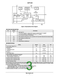
LX
VDD
FB Fault
Protection
TSD
UVLO
PFM
Comparator
Driver
PFM ON/OFF
Timing
−
+
FB
Control
+
−
Vref
Soft−Start
GND
CE
Figure 4. Representative Block Diagram
PIN FUNCTION DESCRIPTION
Pin
Symbol
Description
1
CE
Chip Enable Pin
(1) The chip is enabled if a voltage which is equal to or greater than 0.9 V is applied.
(2) The chip is disabled if a voltage which is less than 0.3 V is applied.
(3) The chip will be enabled if it is left floating.
2
3
4
5
FB
VDD
GND
LX
PFM comparator inverting input, and is connected to off−chip resistor divider which sets output voltage.
Power supply pin for internal circuit.
Ground pin.
External inductor connection pin.
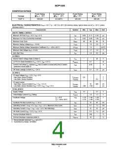
MAXIMUM RATINGS
Rating
Symbol
Value
Unit
Power Supply Voltage (Pin 3)
VDD
−0.3 to 6.0
V
Input/Output Pin
LX (Pin 5)
LX Peak Sink Current
FB (Pin 2)
V
I
−0.3 to 27
1.5
−0.3 to 6.0
V
A
V
LX
LX
V
FB
CE (Pin 1)
Input Voltage Range
V
R
−0.3 to 6.0
V
CE
Power Dissipation and Thermal Characteristics
Maximum Power Dissipation @ T = 25_C
P
D
500
250
mW
_C/W
_C
_C
_C
A
Thermal Resistance, Junction−to−Air
Operating Ambient Temperature Range
Operating Junction Temperature Range
Storage Temperature Range
q
JA
T
−40 to +85
−40 to +150
−55 to +150
A
T
J
T
stg
Maximumratings are those values beyond which device damage can occur. Maximum ratings applied to the device are individual stress limit values
(not normal operating conditions) and are not valid simultaneously. If these limits are exceeded, device functional operation is not implied, damage
may occur and reliability may be affected.
1. This device series contains ESD protection and exceeds the following tests:
Human Body Model (HBM) "2.0 kV per JEDEC standard: JESD22−A114 for all pins.
Machine Model (MM) "200 V per JEDEC standard: JESD22−A115 for all pins.
2. Latchup Current Maximum Rating: "150 mA per JEDEC standard: JESD78.
3. Moisture Sensitivity Level (MSL): 1 per IPC/JEDEC standard: J−STD−020A.
http://onsemi.com
3

 ONSEMI [ ONSEMI ]