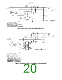
NCP1406
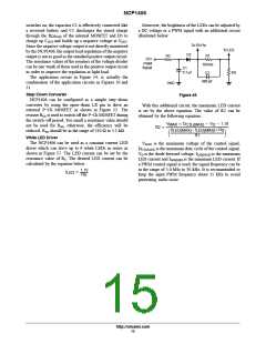
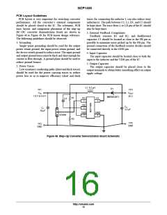
PCB Layout Guidelines
PCB layout is very important for switching converter
performance. All the converter’s external components
should be placed closed to the IC. The schematic, PCB
trace layout, and component placement of the step−up
DC−DC converter demonstration board are shown in
Figure 46 to Figure 49 for PCB layout design reference.
The following guidelines should be observed:
traces for connecting the inductor L can also reduce stray
inductance). The path between C1, L1, D1, and C2 should
be kept short. The trace from L to LX pin of the IC should
also be kept short.
3. External Feedback Components
Feedback resistors R1 and R2, and feedforward
capacitor C3 should be located as close to the FB pin as
possible to minimize noise picked up by the FB pin. The
ground connection of the feedback resistor divider should
be connected directly to the GND pin.
1. Grounding
Single−point grounding should be used for the output
power return ground, the input power return ground, and
the device switch ground to reduce noise. The input ground
and output ground traces must be thick and short enough for
current to flow through. A ground plane should be used to
reduce ground bounce.
4. Input Capacitor
The input capacitor should be located close to both the
input to the inductor and the VDD pin of the IC.
5. Output Capacitor
2. Power Traces
The output capacitor should be placed close to the
output terminals to obtain better smoothing effect on output
ripple voltage.
Low resistance conducting paths (short and thick traces)
should be used for the power carrying traces to reduce
power loss so as to improve efficiency (short and thick
L1 8.2 mH
D1
TP1
TP3
V
IN
V
OUT
1.8 V to 5.0 V
25 V
MBR0530T1
R1
R2
CE
1
LX
5
C3
FB
2
C
2
C
1
3.3 mF
10 mF
VDD
3
GND
4
Enable
TP4
GND
TP2
GND
Figure 46. Step−Up Converter Demonstration Board Schematic
http://onsemi.com
16

 ONSEMI [ ONSEMI ]