NCP1406
Input Capacitor
1% tolerance resistors should be used for both R1 and R2
for better VOUT accuracy.
The input capacitor stabilizes the input voltage and
minimizes peak current ripple from the power source. The
capacitor should be connected directly to the inductor pin
where the input voltage is applied in order to effectively
smooth the input current ripple and voltage due to the
inductor current ripple. The input capacitor is also used to
decouple the high frequency noise from the VDD supply to
the internal control circuit; therefore, the capacitor should
be placed close to the VDD pin. For some particular
applications, separate decoupling capacitors should be
provided and connected directly to the VDD pin for better
decoupling effect. A larger input capacitor can better
reduce ripple current at the input. By reducing the ripple
current at the input, the converter efficiency can be
improved. In general, a 4.7 mF to 22 mF ceramic input
capacitor is sufficient for most applications. X5R and X7R
type ceramic capacitors are recommended due to their
good capacitance tolerance and stable temperature
behavior.
Feedforward Capacitor
A feedforward capacitor is required to add across the
upper feedback resistor to avoid double pulsing or group
pulsing at the switching node which will cause larger
inductor ripple current and higher output voltage ripple.
With adequate feedforward capacitance, evenly distributed
single pulses at the switching node can be achieved. The
range of the capacitor value is from 5.0 pF to 200 pF for
most applications. For NCP1406, the lower the switching
frequency, the larger the feedforward capacitance is
needed; besides, the higher the output voltage, the larger
the feedforward capacitance is required. For the initial trial
value of the feedforward capacitor, the following equation
can be used; however, the actual value needs fine tuning:
1
C
FF
[
f
SW(Load)
2 p
R1
20
Output Voltage Higher than 25 V
Output Capacitor
The NCP1406 can be used to generate output voltage
higher than 25 V by adding an external high voltage N−Ch
MOSFET in series with the internal MOSFET switch as
shown in Figure 51. The drain−to−source breakdown
voltage of the external MOSFET must be at least 1.0 V
higher than the output voltage. The diode D2 connected
across the gate and the source of the external MOSFET
helps the external MOSFET to turn off and ensures that
most of the voltage drops across the external MOSFET
during the switch−off period. Since the high voltage
external MOSFET is in series with the internal MOSFET,
higher break down voltage is achieved but the current
capability is not increased.
There is an alternative application circuit shown in
Figure 53 which can output voltage up to 30 V. For this
circuit, a diode−capacitor charge−pump voltage doubler
constructed by D2, D3 and C1 is added. During the internal
MOSFET switch−on time, the LX pin is shorted to ground
and D2 will charge up C1 to the stepped up voltage at the
cathode of D1. During the MOSFET switch−off time, the
voltage at VOUT will be almost equal to the double of the
voltage at the cathode of D1. The VOUT is monitored by the
FB pin via the resistor divider and can be set by the resistor
values. Since the maximum voltage at the cathode of D1 is
15 V, the maximum VOUT is 30 V. The value of C1 can be in
the range of 0.47 mF to 2.2 mF.
The output capacitor is used for sustaining the output
voltage when no current is delivering from the input, and
smoothing the ripple voltage. Ceramic capacitors should
be used for the output capacitor due to their low ESR at high
switching frequency and low profile in physical size. In
general, a 3.3 mF to 22 mF ceramic capacitor should be
appropriate for most applications. X5R and X7R type
ceramic capacitors are recommended due to their good
capacitance tolerance and temperature coefficient, while
Y5V type ceramic capacitors are not recommended since
both their capacitance tolerance and temperature
coefficient are too large. The output voltage ripple and
switching frequency at nominal load current can be
calculated by the following equations:
I
C
I
L
OUT
OUT SW(Load)
1
PK
ǒ
Ǔ
V
ripple
+
*
f
V
) V −V
IN
OUT
D
* (I −I
PK OUT
) ESR
2I
(V
) V −V
)
IN
OUT OUT
2
D
f
+
SW(Load)
I
L
PK
Where I
is the nominal load current, C
is the
OUT
OUT
selected output capacitance, I
is the peak inductor
PK
current, L is the selected inductance, V
is the output
OUT
voltage, V is the Schottky diode forward voltage, V is
D
IN
the input voltage, ESR is the ESR of the output capacitor.
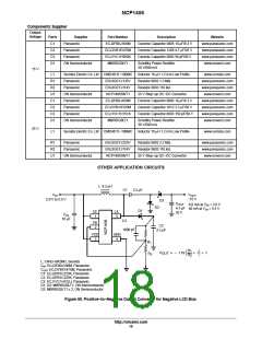
Negative Voltage Generation
The NCP1406 can be used to produce a negative voltage
output by adding a diode−capacitor charge−pump circuit
(D2, D3, and C1) to the LX pin as shown in Figure 50. The
feedback voltage resistor divider is still connected to the
positive output to monitor the positive output voltage and
a small value capacitor is used at C2. When the internal
MOSFET switches off, the voltage at the LX pin charges
up the capacitor through diode D2. When the MOSFET
Feedback Resistors
To achieve better efficiency at light load, a high
impedance feedback resistor divider should be used.
Choose the lower resistor R2 value from the range of 10 kW
to 200 kW. The value of the upper resistor R1 can then be
calculated from the equation below:
V
1.19
OUT
+ R ǒ * 1Ǔ
R
1
2
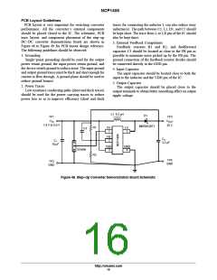
http://onsemi.com
14

 ONSEMI [ ONSEMI ]