NCP1406
APPLICATIONS CIRCUIT INFORMATION
External Component Selection
increases above the maximum output current in DCM
mode. However, stable operation in continuous conduction
mode is hard to achieve, and double pulsing or group
pulsing will occur which will lead to much larger inductor
current ripple and result in larger output ripple voltage.
If the current limit is used to turn off the MOSFET in
order to maximize the output current, it is critical to make
sure that the current limit has been reached before the
maximum on−time is met. To ensure this condition is met,
the inductance L should be selected according the
following inequality:
Inductor
The NCP1406 is designed to work well with a range of
inductance values; the actual inductance value depends on
the specific application, output current, efficiency, and
output ripple voltage. For step−up conversion, the device
works well with inductance ranging from 1.0 mH to 47 mH.
In general, an inductor with small DCR, usually less than
1.0 W, should be used to minimize loss. It is necessary to
choose an inductor with saturation current greater than the
peak switching current in the application.
V
NCP1406 is designed to operate in discontinuous
conduction mode (DCM). Stable operation in continuous
conduction mode is not guaranteed. For each switching
cycle, if the internal MOSFET is switched on, it will be
IN
L t
t
on(max)
I
LIM
Since there is 100 ns internal propagation delay between
the time the current limit is reached and the time the
MOSFET is switched off, the actual peak inductor current
can be obtained from the equation below:
switched off only when either the maximum on−time, t ,
on
of typical 0.9 ms is reached or the inductor current limit of
0.8 A is met, whichever is earlier. Therefore, the designer
can choose to use either the maximum on−time or the
current limit to turn off the MOSFET switch. If the goal is
targeted to minimize output ripple voltage, the maximum
on−time of 0.9 ms should be used to turn off the MOSFET;
however, the maximum output current will be reduced. If
we target to maximize the output current, the current limit
should be chosen to turn off the MOSFET, but this method
will result in a larger output ripple voltage.
V
L
IN
I
+ I
LIM
)
100 ns
PK
Where ILIM is the current limit which is typically 0.8 A,
is the input voltage, L is the selected inductance.
Then the maximum output current under the current limit
control can be calculated by the equation below:
V
IN
V
IN
I
PK
I
+
h
OUT(max)
2(V
) V )
OUT
D
This method can achieve larger maximum output current
in DCM mode. Since the current limit is reached in each
switching cycle, the inductor current ripple is larger
resulting in larger output voltage ripple. Two ceramic
capacitors in parallel can be used at the output to keep the
output ripple small.
If the maximum on−time is used to turn off the MOSFET
in order to achieve a smaller output ripple voltage, it is
critical to ensure that the maximum on−time has been
reached before the current limit is met. To ensure this
condition is met, the inductance L should be selected
according to the following inequality:
Diode
V
IN
L u
t
on(max)
The diode is the main source of loss in DC–DC
converters. The key parameters which affect their
efficiency are the forward voltage drop, V , and the reverse
I
LIM
Where VIN is the input voltage, ILIM is the current limit
which is typically 0.8 A, and t is the maximum
D
on(max)
recovery time, trr. The forward voltage drop creates a loss
just by having a voltage across the device while a current
flowing through it. The reverse recovery time generates a
loss when the diode is reverse biased, and the current
appears to actually flow backwards through the diode due
to the minority carriers being swept from the P–N junction.
A Schottky diode with the following characteristics is
recommended:
on−time which is typically 0.9 ms.
The maximum output current under this maximum
on−time control can be calculated from the equation below:
2
IN
V
t
on(max)
I
+
h
OUT(max)
2L(V
) V )
OUT
D
Where V is the input voltage, t
is the maximum
IN
on(max)
on−time which is typically 0.9 ms, L is the selected
inductance, VOUT is the desired output voltage, V is the
1. Small forward voltage, V < 0.3 V.
D
D
2. Small reverse leakage current.
3. Fast reverse recovery time/switching speed.
4. Rated current larger than peak inductor current,
Schottky diode forward voltage, and h is the conversion
efficiency which can be assumed typically 80% for better
margin for estimation.
The above equation for calculating IOUT(max) is for DCM
mode operation only. In fact, the operation can go beyond
the critical conduction mode if the current loading further
I
> I
.
rated
PK
5. Reverse voltage larger than output voltage,
> V
V
reverse
.
OUT
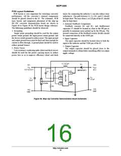
http://onsemi.com
13

 ONSEMI [ ONSEMI ]