NCP1406
DETAILED OPERATING DESCRIPTION
Current Limit
Operation
The NCP1406 is a monolithic DC−DC switching
converter optimized for single Lithium or two cells
AA/AAA size batteries powered portable products.
The NCP1406 device consists of soft−start circuit, chip
enable circuit, PFM comparator, voltage reference, PFM
on/off timing control circuit, driver, current limit circuit,
open−drain MOSFET switch, input voltage UVLO,
thermal shutdown, and feedback pin short−circuit/
open−circuit protection. The device operating current is
typically 15 mA, and can be further reduced to about 0.3 mA
The current limit circuit limits the maximum current
flowing through the LX pin to typical 0.80 A during the
MOSFET switch turn−on period. When the current limit is
exceeded, the switch will be turned off. With the current
limit circuit, the peak inductor current is limited to the
current limit, saturation of inductor is prevented and output
voltage over−shoot during startup can also be minimized.
N−Channel MOSFET Switch
The NCP1406 is built−in with a 26 V open drain
N−Channel MOSFET switch which allows high output
voltage up to 25 V to be generated from simple step−up
topology.
when the chip is disabled (V < 0.3 V).
CE
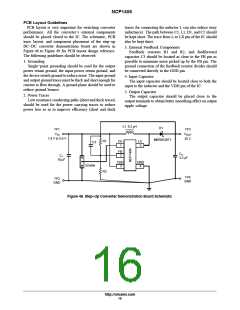
The operation of NCP1406 can be best understood by
referring to the block diagram and typical application
circuit in Figures 1 and 4. The PFM comparator monitors
the output voltage via the external feedback resistor divider
by comparing the feedback voltage with the reference
voltage. When the feedback voltage is lower than the
reference voltage, the PFM control and driver circuit turns
on the N−Channel MOSFET switch and the current ramps
up in the inductor. The switch will remain on for the
maximum on−time, 0.90 ms, or until the current limit is
reached, whichever occurs first. The MOSFET switch is
then turned off and energy stored in the inductor will be
discharged to the output capacitor and load through the
Schottky diode. The MOSFET switch will be turned off for
at least the minimum off−time, 0.13 ms, and will remain off
if the feedback voltage is higher than the reference voltage
and output capacitor will be discharged to sustain the
output current, until the feedback voltage is again lower
than reference voltage. This switching cycle is then
repeated to attain voltage regulation.
Input Voltage Undervoltage Lockout
There is an undervoltage lockout circuit continuously
monitoring the voltage at the VDD pin. The device will be
disabled if the VDD pin voltage drops below the UVLO
threshold voltage.
FB Pin Short−Circuit/Open−Circuit Protection
With the FB protection circuit, the drain−to−source
leakage current of the N−Ch MOSFET is sensed. When the
FB pin connection is shorted or opened, the converter
switches at maximum duty cycle, the peak of V and the
LX
V
OUT
will build up, and the leakage current will increase.
When the leakage current increases to a certain level, the
converter will stop switching with the protection circuit.
Therefore, the peak of V will stop increasing at a certain
LX
level before the N−Ch MOSFET is damaged immediately.
However, the sensing of the leakage current is not very
accurate and cannot be too close to the normal 26 V
maximum operating condition. Therefore, the V
is
LX
around 30 V to 40 V during a FB pin protection fault.
Soft−Start
Thermal Shutdown
There is a soft−start circuit in NCP1406. When power is
applied to the device, the soft−start circuit limits the device
to switch at a small duty cycle initially, the duty cycle is
then increased gradually until the output voltage is in
regulation. With the soft−start circuit, the output voltage
over−shoot is minimized and the startup capability with
heavy loads is also improved.
When the chip junction temperature exceeds 140°C, the
entire IC is shutdown. The IC will resume operation when
the junction temperature drops below 130°C.
Enable/Disable Operation
The NCP1406 offers IC shutdown mode by the chip
enable pin (CE pin) to reduce current consumption. An
internal 150 nA pullup current source ties the CE pin to the
VDD pin by default. Therefore, the user can float the CE
pin for permanent “ON”. When the voltage at the CE pin
is equal to or greater than 0.9 V, the chip will be enabled,
which means the device is in normal operation. When the
voltage at the CE pin is less than 0.3 V, the chip is disabled,
which means IC is shutdown. During shutdown, the IC
supply current reduces to 0.3 mA and the LX pin enters
high impedance state. However, the input remains
connected to the output through the inductor and the
Schottky diode, keeping the output voltage one diode
forward voltage drop below the input voltage.
ON/OFF Timing Control
The maximum on−time is typically 0.90 ms, whereas, the
minimum off−time is typically 0.13 ms. The switching
frequency can be up to 1.0 MHz.
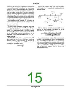
Voltage Reference and Output Voltage
The internal bandgap voltage reference is trimmed to
1.19 V at an accuracy of "1.0% at 25°C. The voltage
reference is connected to the non−inverting input of the
PFM comparator and the inverting input of the PFM
comparator is connected to the FB pin. The output voltage
can be set by connected an external resistor voltage divider
from the VOUT to the FB pin. With the internal 26 V
MOSFET switch, the output voltage can be set between VIN
to 25 V.
http://onsemi.com
12

 ONSEMI [ ONSEMI ]