NCP1399AA, NCP1399BA, NCP1399AC
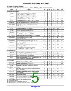
ELECTRICAL CHARACTERISTICS
(For typical values T = 25°C, for min/max values T = −40°C to +125°C, V = 12 V unless otherwise noted.)
J
J
CC
Symbol
Rating
Pin
Min
Typ
Max
Unit
Remote Control – NCP1399Ay (i.e. Off−mode is Sensed via FB Pin)
FB pin voltage above which off−mode is deactivated
V
5
5
5
1.5
0.36
1.0
2.0
0.40
2.3
2.5
0.44
4.0
V
V
FB_REM_ON
(V going up)
FB
V
FB pin voltage below which off−mode is activated
(V going down)
FB
FB_REM_OFF
I
Pull−up FB pin bias current during off−mode
mA
FB_REM_BIAS
Driver Outputs
t
Output voltage rise−time @
C = 1 nF, 10−90% of output signal
L
12, 14
12, 14
20
5
45
30
80
50
ns
ns
r
t
Output voltage fall−time @
f
C = 1 nF, 10−90% of output signal
L
R
Source resistance
12, 14
12, 14
12, 14
4
1
−
16
5
32
11
−
W
W
A
OH
R
Sink resistance
OL
DRVSOURCE
I
Output high short circuit pulsed current
0.5
V
DRV
= 0 V, PW ≤ 10 ms
I
Output high short circuit pulsed current
= VCC, PW ≤ 10 ms
12, 14
−
−
1
−
−
5
A
DRVSINK
V
DRV
I
Leakage current on high voltage pins to GND
14, 15, 16
mA
HV_LEAK
Dead−time Generation
t
Maximum Dead−time value if no dV/dt falling/rising edge is
received
12, 14
720
−
800
8
880
−
ns
−
DEAD_TIME_MAX
N
Number of DT_MAX events to enters IC into fault
(NCP1399AA, NCP1399BA)
12, 14, 16
12, 14, 16
DT_MAX
Number of DT_MAX events to enters IC into fault
(NCP1399AC)
−
16
−
−
dV/dt Detector
P
Positive slew rate on V
dead−time end is generated
pin above which automatic
16
16
−
−
10
10
−
−
V/ms
V/ms
dV/dt_th
BOOT
N
Negative slew rate on V
pin above which automatic
dV/dt_th
BOOT
dead−time end is generated
PFC MODE Output and P ON/OFF Adjust
V
V
PFC MODE output voltage when V < V
P ON/OFF
(sink 1 mA current from PFC MODE output)
9
9
5.75
6.00
−
6.25
−
V
V
PFC_M_BO
PFC_M_ON
PFC_M_LIM
FB
PFC MODE output voltage when V > V
V
0.1
−
FB
P ON/OFF
CC
(sink 10 mA current from PFC MODE output)
I
PFC MODE output current limit (V < 2 V)
9
0.7
9.4
1.2
−
1.85
10.9
mA
s
PFC MODE
t
Delay to transition PFC MODE from V
to
5, 8, 9
P ON/OFF_TIMER
PFC_M_ON
after V drops below V
FB P ON/OFF
V
PFC_M_BO
I
Pull−up current source (Note 4)
8
18
80
20
22
mA
P ON/OFF
P ON/OFF
P ON/OFF comparator hysteresis – percentage level of P
ON/OFF pin voltage
5, 8, 9
100
120
%
HYST
OVP/OTP
V
V
OVP threshold voltage (V
OTP threshold voltage (V
going up)
7
7
2.35
0.76
2.50
0.80
2.65
0.84
V
V
OVP
OVP/OTP
going down)
OTP
OVP/OTP
2. The NCP1399Ay version has skip adjustable externally.
3. Guaranteed by design.
4. Minimal impedance on P ON/OFF pin is 1 kW
5. Minimal resistance connected in series with bootstrap diode is 3.3 W
www.onsemi.com
6

 ONSEMI [ ONSEMI ]