NCP1399AA, NCP1399BA, NCP1399AC
ELECTRICAL CHARACTERISTICS
(For typical values T = 25°C, for min/max values T = −40°C to +125°C, V = 12 V unless otherwise noted.)
J
J
CC
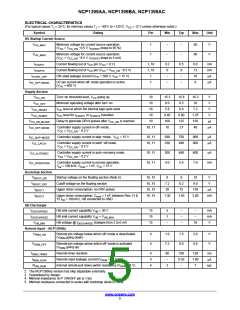
Symbol
HV Startup Current Source
Rating
Pin
Min
Typ
Max
Unit
V
Minimum voltage for current source operation
(V = V −0.5 V, I drops to 95 %)
1
1
−
−
−
−
60
60
V
V
HV_MIN1
CC
CC_ON
START2
V
Minimum voltage for current source operation
(V = V −0.5 V, I drops to 5 mA)
HV_MIN2
CC
CC_ON
START2
I
I
Current flowing out of V pin (V = 0 V)
1, 10
1, 10
1
0.2
6
0.5
9
0.8
13
10
8
mA
mA
mA
START1
CC
CC
Current flowing out of V pin (V = V −0.5 V)
CC_ON
START2
CC
CC
I
Off−state leakage current (V = 500 V, V = 15 V)
−
−
START_OFF
HV
CC
I
HV pin current when off−mode operation is active
(V = 400 V)
1
−
−
mA
HV_OFF−MODE
HV
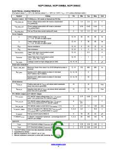
Supply Section
V
Turn−on threshold level, V going up
10
10
15.3
9.0
15.8
9.5
16.3
10
V
V
CC_ON
CC
V
Minimum operating voltage after turn−on
CC_OFF
V
V
V
level at which the internal logic gets reset
10
5.8
6.6
7.2
1.25
150
40
V
CC_RESET
CC_INHIBIT
CC
CC
V
level for I
to I
transition
10
0.40
100
10
0.80
125
27
V
START1
START2
V
Delay to generate DRVs pulses after V
is reached
CC_ON
10
ms
mA
CC_ON_BLANK
CC_OFF−MODE
I
Controller supply current in off−mode,
10, 11
V
CC
= V
− 0.2 V
CC_ON
I
Controller supply current in skip−mode, V = 15 V
10, 11
10, 11
580
330
750
490
900
600
mA
mA
CC_SKIP−MODE
CC
I
Controller supply current in latch−off mode,
CC_LATCH
V
CC
= V
− 0.2 V
CC_ON
I
Controller supply current in auto−recovery mode,
= V − 0.2 V
10, 11
10, 11
300
4.0
490
5.4
600
7.0
mA
CC_AUTOREC
V
CC
CC_ON
I
Controller supply current in normal operation,
= 100 kHz, C = 1 nF, V = 15 V
mA
CC_OPERATION
f
sw
load
CC
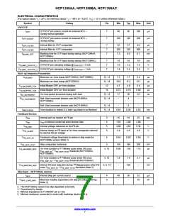
Bootstrap Section
V
Startup voltage on the floating section (Note 5)
Cutoff voltage on the floating section
16, 15
16, 15
16, 15
16, 15
8
9
10
9.0
V
V
BOOT_ON
V
7.2
30
8.2
75
BOOT_OFF
I
I
Upper driver consumption, no DRV pulses
130
2.00
mA
mA
BOOT1
BOOT2
Upper driver consumption, C
= 1 nF between Pins 13 &
1.30
1.65
load
15 f = 100 kHz, HB connected to GND
sw
HB Discharger
I
HB sink current capability V = 30 V
15
15
15
5
1
−
−
−
−
−
−
mA
mA
V
DISCHARGE1
DISCHARGE2
HB
I
HB sink current capability V = V
HB
HB_MIN
V
HB voltage @ I
changes from 2 to 0 mA
10
HB_MIN
DISCHARGE
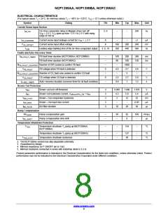
Remote Input – NCP1399By
Remote pin voltage below which off−mode is deactivated
V
4
4
1.0
7.2
1.5
8.0
2.0
8.8
V
V
REM_ON
(V going down)
REM
V
Remote pin voltage above which off−mode is activated
(V going up)
REM_OFF
REM
t
Remote timer duration
4
4
4
80
−
100
0.02
−
120
1.00
7
ms
mA
kW
REM_TIMER
I
Remote input leakage current (V
= 10 V)
REM_LEAK
REM
R
Internal remote pull down switch resistance (V
= 8 V)
REM
3
SW_REM
2. The NCP1399Ay version has skip adjustable externally.
3. Guaranteed by design.
4. Minimal impedance on P ON/OFF pin is 1 kW
5. Minimal resistance connected in series with bootstrap diode is 3.3 W
www.onsemi.com
5

 ONSEMI [ ONSEMI ]