NCP1399AA, NCP1399BA, NCP1399AC
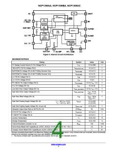
Figure 4. Internal Circuit Architecture
MAXIMUM RATINGS
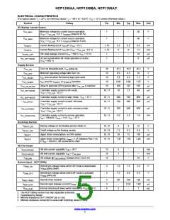
Rating
Symbol
Value
Unit
V
HV Startup Current Source HV Pin Voltage (Pin 1)
VBULK/PFC FB Pin Voltage (Pin3)
V
HV
−0.3 to 600
−0.3 to 5.5
−0.3 to 5.5
−0.3 to 10
−0.3 to 5.5
−5 to 5
V
V
BULK/PFC FB
SKIP/REM Pin Voltage (Pin 4) NCP1399Ay Revision Only
SKIP/REM Pin Voltage (Pin 4) NCP1399By Revision Only
LLC FB Pin Voltage (Pin 5)
V
V
SKIP/REM
V
V
SKIP/REM
V
FB
V
LLC CS Pin Voltage (Pin 6)
V
CS
V
PFC MODE Pin Output Voltage (Pin 9)
VCC Pin Voltage (Pin 10)
V
−0.3 to V + 0.3
V
PFC MODE
CC
V
CC
−0.3 to 20
V
Low Side Driver Output Voltage (Pin 12)
High Side Driver Output Voltage (Pin 14)
V
−0.3 to V + 0.3
V
DRV_MLOWER
CC
V
V
HB
– 0.3 to
V
DRV_MUPPER
V
BOOT
+ 0.3
High Side Offset Voltage (Pin 15)
V
V
V
−20 to
V
V
HB
Boot
+0.3
Boot
High Side Floating Supply Voltage (Pin 16)
T = −40°C to +125°C
J
V
BOOT
−0.3 to 620
−0.3 to 618
J
T = −55°C to −40°C
High Side Floating Supply Voltage (Pin 15 and 16)
Allowable Output Slew Rate on HB Pin (Pin 15)
OVP/OTP Pin Voltage (Pin 7)
V
−0.3 to 20.0
50
V
V/ns
V
Boot–VHB
dV/dt
max
V
−0.3 to 5.5
−0.3 to 5.5
−55 to 150
−55 to 150
130
OVP/OTP
P ON/OFF
P ON/OFF Pin Voltage (Pin 8)
V
V
Junction Temperature
T
J
°C
Storage Temperature
T
STG
°C
Thermal Resistance Junction−to−air
R
°C/W
kV
θ
JA
Human Body Model ESD Capability per JEDEC JESD22−A114F (except HV Pin – Pin 1)
Charged−Device Model ESD Capability per JEDEC JESD22−C101E
−
−
4.5
1
kV
Stresses exceeding those listed in the Maximum Ratings table may damage the device. If any of these limits are exceeded, device functionality
should not be assumed, damage may occur and reliability may be affected.
1. This device contains latch−up protection and exceeds 100 mA per JEDEC Standard JESD78.
www.onsemi.com
4

 ONSEMI [ ONSEMI ]