NPN − MPSA05, MPSA06*;
PNP − MPSA55, MPSA56*
*Preferred Devices
Amplifier Transistors
Voltage and Current are Negative
for PNP Transistors
http://onsemi.com
Features
NPN
PNP
• Pb−Free Packages are Available*
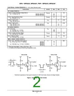
COLLECTOR
3
COLLECTOR
3
MAXIMUM RATINGS
2
2
BASE
BASE
Rating
Symbol
Value
Unit
Collector−Emitter Voltage
V
CEO
V
CBO
V
EBO
Vdc
1
1
MPSA05, MPSA55
MPSA06, MPSA56
60
80
EMITTER
EMITTER
Collector−Base Voltage
Vdc
MPSA05, MPSA55
MPSA06, MPSA56
60
80
Emitter−Base Voltage
4.0
Vdc
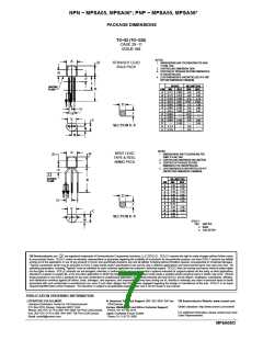
TO−92
Collector Current − Continuous
I
500
mAdc
CASE 29
STYLE 1
C
Total Device Dissipation @ T = 25°C
P
625
5.0
W
mW/°C
A
D
Derate above 25°C
1
1
2
2
Total Device Dissipation @ T = 25°C
P
1.5
12
W
mW/°C
C
D
3
3
Derate above 25°C
STRAIGHT LEAD
BULK PACK
BENT LEAD
TAPE & REEL
AMMO PACK
Operating and Storage Junction
Temperature Range
T , T
J
−55 to +150
°C
stg
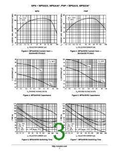
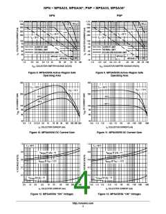
THERMAL CHARACTERISTICS
Characteristic
MARKING DIAGRAM
Symbol
Max
Unit
Thermal Resistance, Junction−to−Ambient
(Note 1)
R
200
°C/W
q
JA
Thermal Resistance, Junction−to−Case
R
83.3
°C/W
q
JC
MPS
Axx
Stresses exceeding Maximum Ratings may damage the device. Maximum
Ratings are stress ratings only. Functional operation above the Recommended
Operating Conditions is not implied. Extended exposure to stresses above the
Recommended Operating Conditions may affect device reliability.
AYWW G
G
1. R
is measured with the device soldered into a typical printed circuit board.
q
JA
xx
A
Y
= 05, 06, 55, or 56
= Assembly Location
= Year
WW = Work Week
G
= Pb−Free Package
(Note: Microdot may be in either location)
ORDERING INFORMATION
See detailed ordering and shipping information in the package
dimensions section on page 6 of this data sheet.
*For additional information on our Pb−Free strategy and soldering details, please
download the ON Semiconductor Soldering and Mounting Techniques
Reference Manual, SOLDERRM/D.
Preferred devices are recommended choices for future use
and best overall value.
© Semiconductor Components Industries, LLC, 2007
1
Publication Order Number:
April, 2007 − Rev. 3
MPSA05/D

 ONSEMI [ ONSEMI ]