MCR12LD, MCR12LM, MCR12LN
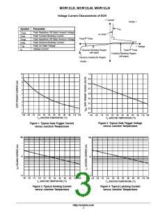
Voltage Current Characteristic of SCR
+ Current
Anode +
V
Symbol
Parameter
TM
V
Peak Repetitive Off State Forward Voltage
Peak Forward Blocking Current
Peak Repetitive Off State Reverse Voltage
Peak Reverse Blocking Current
Peak On State Voltage
DRM
DRM
on state
I
I
H
I
at V
RRM
RRM
V
RRM
I
RRM
V
TM
+ Voltage
I
Holding Current
H
I
at V
DRM
Reverse Blocking Region
(off state)
DRM
Forward Blocking Region
(off state)
Reverse Avalanche Region
Anode −
10
9
1.0
0.9
0.8
0.7
0.6
0.5
0.4
8
7
6
5
4
3
2
1
0
0.3
0.2
−40 −25 −10 5.0 20 35 50 65 80 95 110 125
−40 −25 −10 5.0 20 35 50 65 80 95 110 125
T , JUNCTION TEMPERATURE (°C)
J
T , JUNCTION TEMPERATURE (°C)
J
Figure 2. Typical Gate Trigger Voltage
versus Junction Temperature
Figure 1. Typical Gate Trigger Current
versus Junction Temperature
100
100
10
10
1.0
1.0
−40 −25 −10 5.0 20 35
125
50 65 80 95 110
−40 −25 −10 5.0 20 35
125
65 80 95 110
50
T , JUNCTION TEMPERATURE (°C)
J
T , JUNCTION TEMPERATURE (°C)
J
Figure 3. Typical Holding Current
versus Junction Temperature
Figure 4. Typical Latching Current
versus Junction Temperature
http://onsemi.com
3

 ONSEMI [ ONSEMI ]