MCR12LD, MCR12LM, MCR12LN
THERMAL CHARACTERISTICS
Characteristic
Symbol
Value
Unit
Thermal Resistance,
Junction−to−Case
Junction−to−Ambient
R
R
2.2
62.5
°C/W
q
JC
JA
q
Maximum Lead Temperature for Soldering Purposes 1/8″ from Case for 10 Seconds
T
260
°C
L
ELECTRICAL CHARACTERISTICS (T = 25°C unless otherwise noted)
J
Characteristic
Symbol
Min
Typ
Max
Unit
OFF CHARACTERISTICS
Peak Repetitive Forward or Reverse Blocking Current
(V = Rated V and V ; Gate Open)
T = 25°C
T = 125°C
J
I
,
DRM
−
−
−
−
0.01
2.0
mA
J
I
RRM
D
DRM
RRM
ON CHARACTERISTICS
Peak Forward On−State Voltage (Note 2)
V
−
−
2.2
8.0
20
V
TM
(I = 24 A)
TM
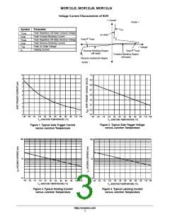
Gate Trigger Current (Continuous dc)
I
2.0
4.0
4.0
10
mA
mA
GT
(V = 12 V, R = 100 W)
D
L
Holding Current
I
H
(V = 12 V, Gate Open, Initiating Current = 200 mA)
D
Latch Current (V = 12 V, Ig = 20 mA)
I
6.0
0.5
12
30
mA
V
D
L
Gate Trigger Voltage (Continuous dc)
V
0.65
0.8
GT
(V = 12 V, R = 100 W)
D
L
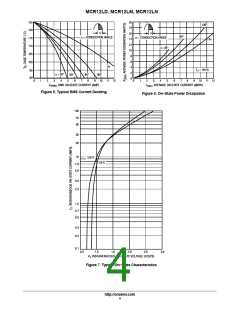
DYNAMIC CHARACTERISTICS
Critical Rate of Rise of Off−State Voltage
dv/dt
di/dt
100
−
250
−
−
V/ms
A/ms
(V = Rated V
, Exponential Waveform, Gate Open, T = 125°C)
DRM J
D
Critical Rate of Rise of On−State Current
50
IPK = 50 A; Pw = 40 msec; diG/dt = 1 A/msec, Igt = 50 mA
2. Indicates Pulse Test: Pulse Width v1.0 ms, Duty Cycle v2%.
http://onsemi.com
2

 ONSEMI [ ONSEMI ]