MC7800, MC7800A, NCV7805
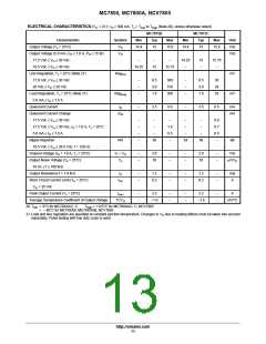
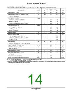
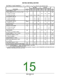
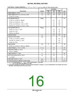
ELECTRICAL CHARACTERISTICS (V = 33 V, I = 500 mA, T = T to T (Note 28), unless otherwise noted)
high
in
O
J
low
MC7824B
Typ
MC7824C
Typ
Characteristic
Output Voltage (T = 25°C)
Symbol
Min
Max
Min
Max
Unit
Vdc
Vdc
V
O
V
O
23
24
25
23
24
25
J
Output Voltage (5.0 mA ≤ I ≤ 1.0 A, P ≤ 15 W)
O
D
27 Vdc ≤ V ≤ 38 Vdc
−
−
−
22.8
−
24
−
25.2
−
in
28 Vdc ≤ V ≤ 38 Vdc
22.8
24
25.2
in
Line Regulation, (Note 29)
Reg
mV
mV
line
27 Vdc ≤ V ≤ 38 Vdc
−
−
−
11.5
3.8
480
240
480
−
−
−
2.7
2.7
4.4
60
48
65
in
30 Vdc ≤ V ≤ 36 Vdc
in
Load Regulation, (Note 29)
Reg
2.1
load
5.0 mA ≤ I ≤ 1.5 A
O
Quiescent Current
I
−
3.6
8.0
−
3.6
6.5
mA
mA
B
Quiescent Current Change
DI
B
27 Vdc ≤ V ≤ 38 Vdc
−
−
−
−
−
−
0.5
−
−
−
−
−
1.0
0.5
−
in
5.0 mA ≤ I ≤ 1.0 A
O
Ripple Rejection
RR
54
50
54
dB
28 Vdc ≤ V ≤ 38 Vdc, f = 120 Hz
in
Dropout Voltage (I = 1.0 A, T = 25°C)
V − V
O
−
−
2.0
10
−
−
−
−
2.0
10
−
−
Vdc
O
J
I
Output Noise Voltage (T = 25°C)
V
n
mV/V
O
A
10 Hz ≤ f ≤ 100 kHz
Output Resistance f = 1.0 kHz
r
−
−
1.4
0.2
−
−
−
−
1.4
0.2
−
−
mW
O
Short Circuit Current Limit (T = 25°C)
I
A
A
SC
V
in
= 35 Vdc
Peak Output Current (T = 25°C)
I
−
−
2.2
−
−
−
−
2.2
−
−
A
J
max
Average Temperature Coefficient of Output Voltage
TCV
−2.0
−2.0
mV/°C
O
28.T
= 0°C for MC78XXAC, C
T
high
= +125°C for MC78XXAC, C, NCV7805
low
= *40°C for MC78XXB, MC78XXAB, NCV7805
29.Load and line regulation are specified at constant junction temperature. Changes in V due to heating effects must be taken into account
O
separately. Pulse testing with low duty cycle is used.
http://onsemi.com
17

 ONSEMI [ ONSEMI ]