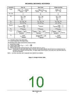
MC34063A, MC33063A, NCV33063A
Calculation
/t
Step−Up
Step−Down
Voltage−Inverting
t
V
) V * V
V
) V
|V | ) V
on off
out
out
out
F
F
in(min)
sat
F
V
* V
* V
V
* V
V
* V
sat
out
sat
in(min)
in
in(min)
(t + t
on
)
off
1
f
1
f
1
f
t
t
) t
t
) t
t
) t
off
on
t
on
on
t
off
off
) 1
off
t
t
on
on
off
on
) 1
) 1
t
t
off
(t + t ) − t
off
(t + t ) − t
off
t
(t + t ) − t
on
on
on
off
off
off
off
on
off
−5
−5
−5
C
T
4.0 x 10
t
4.0 x 10
t
4.0 x 10
t
on
on
on
I
pk(switch)
t
t
t
t
on
off
on
off
2I
2I
ǒ
) 1
Ǔ
2I
ǒ
) 1
Ǔ
out(max)
out(max)
0.3/I
out(max)
0.3/I
R
sc
0.3/I
pk(switch)
pk(switch)
pk(switch)
L
(min)
(V
* V
)
(V
* V
* V
)
(V
* V
)
sat
sat
pk(switch)
out
sat
in(min)
I
in(min)
I
in(min)
I
t
t
t
ǒ
Ǔ ǒ
Ǔ ǒ
Ǔ
on(max)
on(max)
on(max)
pk(switch)
pk(switch)
C
I
t
I
(t
) t
)
I
t
O
on
on
on
out
out
pk(switch)
8V
off
9
9
V
V
ripple(pp)
ripple(pp)
ripple(pp)
V
V
= Saturation voltage of the output switch.
= Forward voltage drop of the output rectifier.
sat
F
The following power supply characteristics must be chosen:
V
− Nominal input voltage.
|V
− Desired output voltage,
− Desired output current.
− Minimum desired output switching frequency at the selected values of V and I .
in
R2
R1
| + 1.25 ǒ1 )
Ǔ
V
out
out
I
f
out
min
in
O
V
− Desired peak−to−peak output ripple voltage. In practice, the calculated capacitor value will need to be increased due to its
equivalent series resistance and board layout. The ripple voltage should be kept to a low value since it will directly affect the
line and load regulation.
ripple(pp)
NOTE: For further information refer to Application Note AN920A/D and AN954/D.
Figure 15. Design Formula Table
http://onsemi.com
10

 ONSEMI [ ONSEMI ]