MC34071,2,4,A MC33071,2,4,A
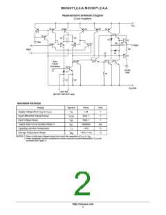
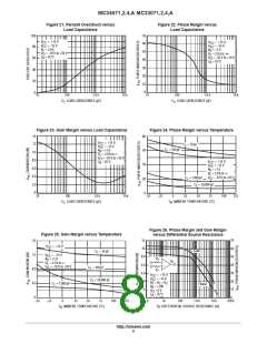
Representative Schematic Diagram
(Each Amplifier)
V
CC
Q3
Q8
Q4
Q6
Q5
Q7
Q1
Q17
Q2
R2
R1
C1
D2
Q18
Bias
R6
R7
Q11
Q9
Q10
Output
–
R8
Inputs
+
C2
D3
Q19
Q15
Q16
Q13
R4
Q14
Base
Current
Cancellation
Q12
D1
Current
Limit
R5
R3
V /Gnd
EE
Offset Null
(MC33071, MC34071 only)
MAXIMUM RATINGS
Rating
Supply Voltage (from V
Symbol
Value
+44
Unit
V
to V
)
V
S
EE
CC
Input Differential Voltage Range
Input Voltage Range
V
Note 1
Note 1
V
IDR
V
V
IR
Output Short Circuit Duration (Note 2)
Operating Junction Temperature
Storage Temperature Range
t
Indefinite
+150
sec
°C
°C
SC
T
J
T
–60 to +150
stg
NOTES: 1. Either or both input voltages should not exceed the magnitude of V
or V .
EE
CC
2. Power dissipation must be considered to ensure maximum junction temperature (T ) is not
J
exceeded (see Figure 1).
http://onsemi.com
2

 ONSEMI [ ONSEMI ]