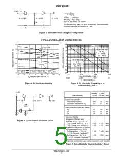
MC14060B
SWITCHING CHARACTERISTICS (C = 50 pF, T = 25 C)
L
A
V
Vdc
DD
(7.)
Characteristic
Symbol
Min
Typ
Max
Unit
Output Rise Time (Counter Outputs)
t
5.0
10
15
—
—
—
40
25
20
200
100
80
ns
TLH
Output Fall Time (Counter Outputs)
t
5.0
10
15
—
—
—
50
30
20
200
100
80
ns
ns
THL
Propagation Delay Time
Clock to Q4
t
t
5.0
10
15
—
—
—
415
175
125
740
300
200
PLH
PHL
5.0
10
15
—
—
—
1.5
0.7
0.4
2.7
1.3
1.0
µs
Clock to Q14
Clock Pulse Width
t
5.0
10
15
100
40
30
65
30
20
—
—
—
ns
wH
Clock Pulse Frequency
Clock Rise and Fall Time
Reset Pulse Width
f
5.0
10
15
—
—
—
5
14
17
3.5
8
12
MHz
ns
φ
t
t
5.0
10
15
TLH
THL
No Limit
t
w
5.0
10
15
120
60
40
40
15
10
ns
—
—
—
Propagation Delay Time
Reset to On
t
5.0
10
15
—
—
—
170
80
60
350
160
100
ns
PHL
7. Data labelled “Typ” is not to be used for design purposes but is intended as an indication of the IC’s potential performance.
V
DD
V
DD
CLOCK
NC OUT1
PULSE
GENERATOR
500 µF
0.01 µF
I
D
Q4
Q5
Qn
NC OUT2
C
L
R
C
L
CLOCK
PULSE
GENERATOR
Q4
C
L
V
SS
NC OUT1 Q5
NC OUT2
Qn
C
L
R
20 ns
20 ns
C
L
C
L
V
SS
90%
50%
10%
CLOCK
t
WH
20 ns
20 ns
t
t
PHL
PLH
V
DD
90%
90%
50%
10%
50%
10%
CLOCK
Q
V
SS
t
t
THL
50% DUTY CYCLE
TLH
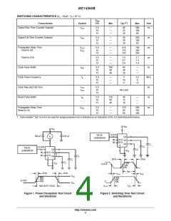
Figure 1. Power Dissipation Test Circuit
and Waveform
Figure 2. Switching Time Test Circuit
and Waveforms
http://onsemi.com
4

 ONSEMI [ ONSEMI ]