MAC12HCD, MAC12HCM, MAC12HCN
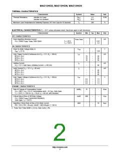
THERMAL CHARACTERISTICS
Characteristic
Symbol
Value
Unit
Thermal Resistance,
Junction−to−Case
Junction−to−Ambient
R
R
2.2
62.5
°C/W
q
JC
JA
q
Maximum Lead Temperature for Soldering Purposes 1/8″ from Case for 10 Seconds
T
260
°C
L
ELECTRICAL CHARACTERISTICS (T = 25°C unless otherwise noted; Electricals apply in both directions)
J
Characteristic
Symbol
Min
Typ
Max
Unit
OFF CHARACTERISTICS
Peak Repetitive Blocking Current
I
, I
mA
DRM RRM
(V = Rated V
, V
DRM
, Gate Open)
RRM
T = 25°C
T = 125°C
J
−
−
−
−
0.01
2.0
D
J
ON CHARACTERISTICS
Peak On-State Voltage (Note 2)
(I 17 A)
Gate Trigger Current (Continuous dc) (V = 12 V, R = 100 W)
V
V
TM
=
−
−
1.85
TM
I
mA
D
L
GT
MT2(+), G(+)
MT2(+), G(−)
MT2(−), G(−)
10
10
10
−
−
−
50
50
50
Holding Current
(V = 12 V, Gate Open, Initiating Current = 150 mA)
D
I
mA
mA
H
−
−
60
Latch Current (V = 12 V, I = 50 mA)
I
D
G
L
MT2(+), G(+)
MT2(+), G(−)
MT2(−), G(−)
−
−
−
−
−
−
60
80
60
Gate Trigger Voltage (Continuous dc) (V = 12 V, R = 100 W)
V
V
D
L
GT
MT2(+), G(+)
MT2(+), G(−)
MT2(−), G(−)
0.5
0.5
0.5
−
−
−
1.5
1.5
1.5
DYNAMIC CHARACTERISTICS
Rate of Change of Commutating Current
(V = 400 V, I = 4.4 A, Commutating dv/dt = 18 V/ms, Gate Open,
(di/dt)
dv/dt
di/dt
15
600
−
−
−
−
−
−
A/ms
V/ms
A/ms
c
D
TM
T = 125°C, f = 250 Hz, C = 10 mF, L = 40 mH, with Snubber)
J
L
L
Critical Rate of Rise of Off-State Voltage
(V = Rated V , Exponential Waveform,
D
DRM
Gate Open, T = 125°C)
J
Repetitive Critical Rate of Rise of On-State Current
10
IPK = 50 A; PW = 40 msec; diG/dt = 200 mA/msec; f = 60 Hz
2. Pulse Test: Pulse Width ≤ 2.0 ms, Duty Cycle ≤ 2%.
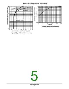
http://onsemi.com
2

 ONSEMI [ ONSEMI ]