ESDR0502B
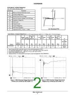
ELECTRICAL CHARACTERISTICS
(T = 25°C unless otherwise noted)
A
I
Symbol
Parameter
Maximum Reverse Peak Pulse Current
Clamping Voltage @ I
I
F
I
PP
V
C
PP
V
RWM
Working Peak Reverse Voltage
V
C
V
V
BR RWM
I
Maximum Reverse Leakage Current @ V
V
R
RWM
I
V
F
R
T
I
V
BR
Breakdown Voltage @ I
Test Current
T
I
T
I
F
Forward Current
I
PP
V
F
Forward Voltage @ I
F
P
Peak Power Dissipation
Capacitance @ V = 0 and f = 1.0 MHz
pk
Uni−Directional TVS
C
R
ELECTRICAL CHARACTERISTICS (T = 25°C unless otherwise noted, V = 1.1 V Max. @ I = 10 mA for all types)
A
F
F
V
(V)
C (pF),
uni−directional
(Note 3)
C (pF),
bi−directional
(Note 4)
V (V)
C
BR
V
I
(mA)
@ I
@ I = 1 A
RWM
(V)
R
T
PP
@ V
(Note 2)
(Note 5)
I
T
V
C
RWM
Per
IEC61000−
4−2
Device
Max
Max
1.0
Min
mA
Typ
Max
Typ
Max
Max
(Note 6)
Marking
Device
ESDR0502B
AD
5.0
5.8
1.0
0.5
0.9
0.25
0.45
15
Figures 1
and 2
2. V is measured with a pulse test current I at an ambient temperature of 25°C.
BR
T
3. Uni−directional capacitance at f = 1 MHz, V = 0 V, T = 25°C (pin1 to pin 3; pin 2 to pin 3).
R
A
4. Bi−directional capacitance at f = 1 MHz, V = 0 V, T = 25°C (pin1 to pin 2).
R
A
5. Surge current waveform per Figure 5.
6. Typical waveform. For test procedure see Figures 3 and 4 and Application Note AND8307/D.
Figure 2. ESD Clamping Voltage Screenshot
Figure 1. ESD Clamping Voltage Screenshot
Negative 8 kV contact per IEC 61000−4−2
Positive 8 kV contact per IEC 61000−4−2
http://onsemi.com
2

 ONSEMI [ ONSEMI ]