BTB16−600BW3G, BTB16−700BW3G, BTB16−800BW3G
THERMAL CHARACTERISTICS
Characteristic
Symbol
Value
Unit
Thermal Resistance,
Junction−to−Case (AC)
Junction−to−Ambient
R
R
1.9
60
°C/W
q
JC
q
JA
Maximum Lead Temperature for Soldering Purposes 1/8″ from Case for 10 seconds
T
L
260
°C
ELECTRICAL CHARACTERISTICS (T = 25°C unless otherwise noted; Electricals apply in both directions)
J
Characteristic
Symbol
Min
Typ
Max
Unit
OFF CHARACTERISTICS
Peak Repetitive Blocking Current
I
/
mA
DRM
(V = Rated V
, V
RRM
; Gate Open)
T = 25°C
T = 125°C
J
I
−
−
−
−
0.005
2.0
D
DRM
J
RRM
ON CHARACTERISTICS
Peak On-State Voltage (Note 2)
(I 22.5 A Peak)
Gate Trigger Current (Continuous dc) (V = 12 V, R = 30 W)
V
−
−
1.55
V
TM
=
TM
I
mA
D
L
GT
MT2(+), G(+)
MT2(+), G(−)
MT2(−), G(−)
2.5
2.5
2.5
−
−
−
50
50
50
Holding Current
(V = 12 V, Gate Open, Initiating Current = 150 mA)
D
I
−
−
60
mA
mA
H
Latching Current (V = 12 V, I = 50 mA)
I
D
G
L
MT2(+), G(+)
MT2(+), G(−)
MT2(−), G(−)
−
−
−
−
−
−
70
90
70
Gate Trigger Voltage (V = 12 V, R = 30 W)
V
V
V
D
L
GT
MT2(+), G(+)
MT2(+), G(−)
MT2(−), G(−)
0.5
0.5
0.5
−
−
−
1.7
1.1
1.1
Gate Non−Trigger Voltage (T = 125°C)
V
GD
J
MT2(+), G(+)
MT2(+), G(−)
MT2(−), G(−)
0.2
0.2
0.2
−
−
−
−
−
−
DYNAMIC CHARACTERISTICS
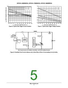
Rate of Change of Commutating Current, See Figure 10.
(dI/dt)
dI/dt
7.5
−
−
−
−
−
50
−
A/ms
A/ms
V/ms
c
(Gate Open, T = 125°C, No Snubber)
J
Critical Rate of Rise of On−State Current
(T = 125°C, f = 120 Hz, I = 2 x I , tr ≤ 100 ns)
J
G
GT
Critical Rate of Rise of Off-State Voltage
(V = 0.66 x V , Exponential Waveform, Gate Open, T = 125°C)
dV/dt
1500
D
DRM
J
2. Indicates Pulse Test: Pulse Width ≤ 2.0 ms, Duty Cycle ≤ 2%.
http://onsemi.com
2

 ONSEMI [ ONSEMI ]