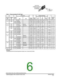
1.0
0.7
0.5
D = 0.5
0.2
0.3
0.2
0.1
P
(pk)
0.05
0.02
0.1
0.07
0.05
R
(t) = r(t) R
= 1.92°C/W
θJC θJC
R
θJC
D CURVES APPLY FOR POWER
PULSE TRAIN SHOWN
READ TIME AT t
t
1
SINGLE
PULSE
0.03
0.02
t
2
SINGLE PULSE
1
0.01
T
J(pk)
– T = P
C
R
(t)
(pk) θJC
DUTY CYCLE, D = t /t
1 2
0.01
0.01 0.02 0.03 0.05
0.1
0.2 0.3 0.5
1.0
2.0 3.0 5.0
10
20 30
50
100
200 300 500
1000
t, TIME OR PULSE WIDTH (ms)
Figure 4. Thermal Response
20
10
100 µs
500 µs
There are two limitations on the power handling ability of a
transistor average junction temperature and second break-
5.0
down. Safe operating area curves indicate I –V
limits of
C
CE
5.0 ms
1.0 ms
the transistor that must be observed for reliable operation,
i.e., the transistor must not be subjected to greater dissipa-
tion than the curves indicate.
dc
2.0
1.0
0.5
T = 150°C
J
BONDING WIRE LIMITED
THERMALLY LIMITED @ T = 25°C
(SINGLE PULSE)
SECOND BREAKDOWN LIMITED
C
The data of Figure 5 is based on T
J(pk)
= 150 C; T is
C
variable depending on conditions. Second breakdown pulse
limits are valid for duty cycles to 10% provided T
0.2
0.1
J(pk)
may be calculated from the data in Fig-
CURVES APPLY BELOW RATED V
CEO
150 C. T
J(pk)
ure 4. At high case temperatures, thermal limitations will
reduce the power that can be handled to values less than the
limitations imposed by second breakdown.
0.05
BDX53B, BDX54B
BDX53C, BDX54C
0.02
1.0
2.0 3.0
5.0 7.0 10
20 30
50 70 100
V , COLLECTOR–EMITTER VOLTAGE (VOLTS)
CE
Figure 5. Active–Region Safe Operating Area
10,000
5000
300
T = + 25°C
J
3000
2000
200
1000
500
300
200
C
ob
100
70
T = 25°C
J
V
= 3.0 V
CE
= 3.0 A
C
ib
I
100
C
50
30
20
50
PNP
NPN
PNP
NPN
10
30
1.0
2.0
5.0 10
20
50 100 200
500 1000
0.1
0.2
0.5 1.0 2.0
5.0 10
20
50 100
V , REVERSE VOLTAGE (VOLTS)
R
f, FREQUENCY (kHz)
Figure 6. Small-Signal Current Gain
Figure 7. Capacitance
3–223
Motorola Bipolar Power Transistor Device Data

 ONSEMI [ ONSEMI ]