FEDL66517-01
1
Semiconductor
ML66517 Family
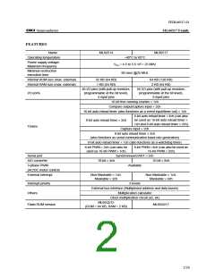
FEATURES
Name
ML66514
ML66517
Operating temperature
–40°C to 85°C
Power supply voltage/
Maximum frequency
VDD = 4.5 to 5.5 V/f = 25 MHz
Minimum instruction
execution time
80 nsec @25 MHz
Internal ROM size (max. external)
Internal RAM size (max. external)
32 KB (64 KB)
1 KB (64 KB)
64 KB (128 KB)
2 KB (64 KB)
46 I/O pins (with pull-up resistors,
programmable at the bit level),
4 input pins
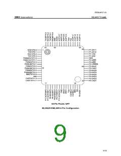
56 I/O pins (with pull-up resistors,
programmable at the bit level),
8 input pins
I/O ports
16-bit free-running counter × 1ch
Compare output/capture input × 2ch
16-bit auto-reload timer (also functions as a event input/timer out) × 1ch
8-bit auto reload timer × 4ch (can also
8-bit auto reload timer × 2ch
be used as 16-bit auto reload timer ×
1ch and 8-bit auto reload timer × 2ch)
Timers
Capture input × 2ch
8-bit auto reload timer × 2ch
(also functions as serial communication baud rate generators)
8-bit auto reload timer × 1ch (also functions as a watchdog timer)
8-bit PWM × 2ch (can also be
used as 16-bit PWM × 1ch)
8-bit PWM × 4ch (can also be used as
16-bit PWM × 2ch)
Serial port
Synchronous/UART × 2ch
A/D converter
10-bit × 4ch
10-bit × 8ch
3-phase PWM
(AC/DC motor control)
External interrupt
Available
Non-Maskable × 1ch;
Maskable × 2ch
Non-Maskable × 1ch;
Maskable × 4ch
Interrupt priority
Others
3 levels
External bus interface (Multiplexed address and data buses)
Multiplication calculator
Clock multiplication circuit (x2, x4)
ML66Q515
ML66Q517
Flash ROM version
(ROM = 64 KB, RAM = 2 KB)
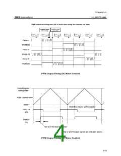
2/29

 OKI [ OKI ELECTRONIC COMPONETS ]