FEDL66517-01
1
Semiconductor
ML66517 Family
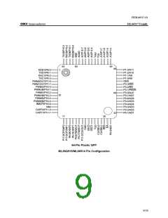
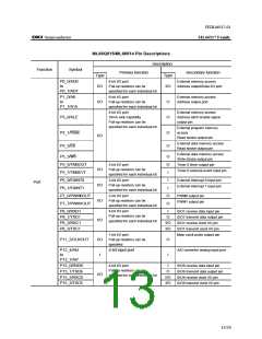
ML66Q515/ML66514 Pin Descriptions
Description
Function
Symbol
Primary function
Secondary function
Type
I/O
Type
I/O
P0_0/AD0
8-bit I/O port
External memory access
to
Pull-up resistors can be
specified for each individual bit
Address output/Data I/O port
P0_7/AD7
P1_0/A8
to
P1_7/A15
8-bit I/O port
External memory access
Address output port
I/O
Pull-up resistors can be
specified for each individual bit
O
O
4-bit I/O port
External memory access
Address latch enable signal
output pin
P3_0/ALE
10mA sink capability
Pull-up resistors can be
specified for each individual bit
External program memory
access
P3_1/PSEN
P3_2/RD
O
O
I/O
Read strobe output pin
External data memory access
Read strobe output pin
External data memory access
Write strobe output pin
P3_3/WR
O
O
I
P5_6/TM0OUT
P5_7/TM0EVT
P6_0/EXINT0
P6_1/EXINT1
P7_6/PWM0OUT
P7_7/PWM1OUT
2-bit I/O port
Timer 0 timer output pin
I/O
I/O
I/O
Pull-up resistors can be
specified for each individual bit
Timer 0 external event input pin
2-bit I/O port
I
External interrupt 0 input pin
External interrupt 1 input pin
Port
Pull-up resistors can be
specified for each individual bit
I
2-bit I/O port
O
O
PWM0 output pin
PWM1 output pin
Pull-up resistors can be
specified for each individual bit
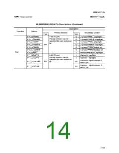
P8_0/RXD1
P8_1/TXD1
P8_2/RXC1
P8_3/TXC1
4-bit I/O port
I
SIO1 receive data input pin
SIO1 transmit data output pin
SIO1 receive clock I/O pin
SIO1 transmit clock I/O pin
Main clock pulse output pin
Pull-up resistors can be
specified for each individual bit
O
I/O
I/O
I/O
1-bit I/O port
P11_2/CLKOUT
I/O
I
Pull-up resistors can be
specified
O
I
P12_4/AI4
to
4-bit input port
A/D converter analog input port
P12_7/AI7
P15_0/RXD6
P15_1/TXD6
P15_2/RXC6
P15_3/TXC6
4-bit I/O port
I
SIO6 receive data input pin
SIO6 transmit data output pin
SIO6 receive clock I/O pin
SIO6 transmit clock I/O pin
Pull-up resistors can be
specified for each individual bit
O
I/O
I/O
I/O
13/29

 OKI [ OKI ELECTRONIC COMPONETS ]