TJA1028
NXP Semiconductors
LIN transceiver with integrated voltage regulator
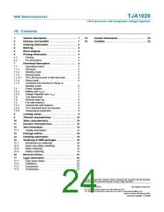
19. Contents
1
2
3
4
5
General description. . . . . . . . . . . . . . . . . . . . . . 1
18
19
Contact information . . . . . . . . . . . . . . . . . . . . 23
Contents. . . . . . . . . . . . . . . . . . . . . . . . . . . . . . 24
Features and benefits . . . . . . . . . . . . . . . . . . . . 1
Ordering information. . . . . . . . . . . . . . . . . . . . . 2
Marking. . . . . . . . . . . . . . . . . . . . . . . . . . . . . . . . 2
Block diagram . . . . . . . . . . . . . . . . . . . . . . . . . . 3
6
6.1
6.2
Pinning information. . . . . . . . . . . . . . . . . . . . . . 4
Pinning . . . . . . . . . . . . . . . . . . . . . . . . . . . . . . . 4
Pin description . . . . . . . . . . . . . . . . . . . . . . . . . 4
7
7.1
Functional description . . . . . . . . . . . . . . . . . . . 4
Operating modes . . . . . . . . . . . . . . . . . . . . . . . 5
Off mode. . . . . . . . . . . . . . . . . . . . . . . . . . . . . . 5
Standby mode. . . . . . . . . . . . . . . . . . . . . . . . . . 5
Normal mode . . . . . . . . . . . . . . . . . . . . . . . . . . 6
The LIN transceiver in Normal mode . . . . . . . . 6
Sleep mode . . . . . . . . . . . . . . . . . . . . . . . . . . . 6
Transition from Normal to Sleep or
7.1.1
7.1.2
7.1.3
7.1.3.1
7.1.4
7.1.5
Standby mode. . . . . . . . . . . . . . . . . . . . . . . . . . 6
Power supplies . . . . . . . . . . . . . . . . . . . . . . . . . 7
Battery (pin VBAT) . . . . . . . . . . . . . . . . . . . . . . . 7
Voltage regulator (pin VCC). . . . . . . . . . . . . . . . 7
LIN transceiver . . . . . . . . . . . . . . . . . . . . . . . . 7
Remote wake-up . . . . . . . . . . . . . . . . . . . . . . . 8
Fail-safe features . . . . . . . . . . . . . . . . . . . . . . . 8
General fail-safe features . . . . . . . . . . . . . . . . . 8
TXD dominant time-out function. . . . . . . . . . . . 8
Temperature protection. . . . . . . . . . . . . . . . . . . 9
7.2
7.2.1
7.2.2
7.3
7.4
7.5
7.5.1
7.5.2
7.5.3
8
Limiting values. . . . . . . . . . . . . . . . . . . . . . . . . . 9
Thermal characteristics . . . . . . . . . . . . . . . . . 10
Static characteristics. . . . . . . . . . . . . . . . . . . . 10
Dynamic characteristics . . . . . . . . . . . . . . . . . 13
Test information. . . . . . . . . . . . . . . . . . . . . . . . 15
Quality information . . . . . . . . . . . . . . . . . . . . . 15
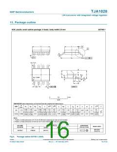
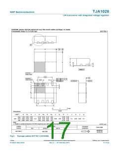
Package outline . . . . . . . . . . . . . . . . . . . . . . . . 16
Handling information. . . . . . . . . . . . . . . . . . . . 18
9
10
11
12
12.1
13
14
15
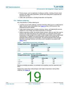
Soldering of SMD packages . . . . . . . . . . . . . . 18
Introduction to soldering . . . . . . . . . . . . . . . . . 18
Wave and reflow soldering . . . . . . . . . . . . . . . 18
Wave soldering. . . . . . . . . . . . . . . . . . . . . . . . 18
Reflow soldering. . . . . . . . . . . . . . . . . . . . . . . 19
15.1
15.2
15.3
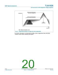
15.4
16
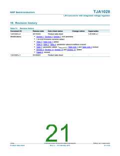
Revision history. . . . . . . . . . . . . . . . . . . . . . . . 21
17
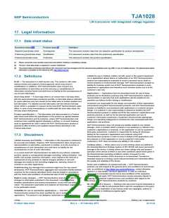
Legal information. . . . . . . . . . . . . . . . . . . . . . . 22
Data sheet status . . . . . . . . . . . . . . . . . . . . . . 22
Definitions. . . . . . . . . . . . . . . . . . . . . . . . . . . . 22
Disclaimers. . . . . . . . . . . . . . . . . . . . . . . . . . . 22
Trademarks. . . . . . . . . . . . . . . . . . . . . . . . . . . 23
17.1
17.2
17.3
17.4
Please be aware that important notices concerning this document and the product(s)
described herein, have been included in section ‘Legal information’.
© NXP B.V. 2011.
All rights reserved.
For more information, please visit: http://www.nxp.com
For sales office addresses, please send an email to: salesaddresses@nxp.com
Date of release: 25 February 2011
Document identifier: TJA1028

 NXP [ NXP ]