LPC546xx
NXP Semiconductors
32-bit ARM Cortex-M4 microcontroller
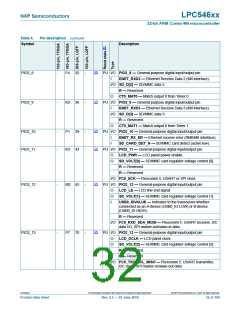
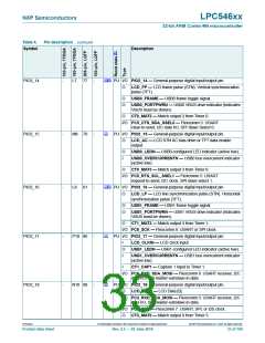
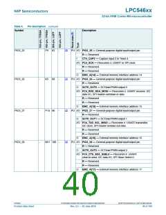
Table 4.
Symbol
Pin description …continued
Description
[2]
PIO3_1
PIO3_2
-
-
D11 159
-
-
PU I/O PIO3_1 — General-purpose digital input/output pin.
O
I
LCD_VD[15] — LCD Data [15].
PDM0_DATA — Data for PDM interface 0 (digital
microphone).
R — Reserved.
O
CT1_MAT1 — Match output 1 from Timer 1.
[2]
C10 164
PU I/O PIO3_2 — General-purpose digital input/output pin.
LCD_VD[16] — LCD Data [16].
O
I/O FC9_RXD_SDA_MOSI — Flexcomm 9: USART receiver, I2C
data I/O, SPI master-out/slave-in data.
R — Reserved.
O
CT1_MAT2 — Match output 2 from Timer 1.
PU I/O PIO3_3 — General-purpose digital input/output pin.
LCD_VD[17] — LCD Data [17].
[2]
[2]
PIO3_3
PIO3_4
-
-
A13 169
B11 172
-
-
O
I/O FC9_TXD_SCL_MISO — Flexcomm 9: USART transmitter,
I2C clock, SPI master-in/slave-out data.
PU I/O PIO3_4 — General-purpose digital input/output pin.
O
LCD_VD[18] — LCD Data [18].
R — Reserved.
I/O FC8_CTS_SDA_SSEL0 — Flexcomm 8: USART
clear-to-send, I2C data I/O, SPI Slave Select 0.
I
CT4_CAP1 — Capture input 4 to Timer 1.
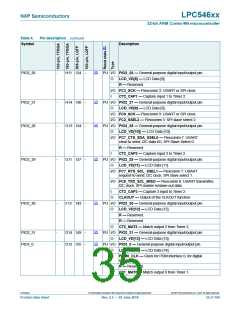
[2]
PIO3_5
-
B10 177
-
PU I/O PIO3_5 — General-purpose digital input/output pin.
O
LCD_VD[19] — LCD Data [19].
R — Reserved.
I/O FC8_RTS_SCL_SSEL1 — Flexcomm 8: USART
request-to-send, I2C clock, SPI slave select 1.
O
CT4_MAT1 — Match output 1 from Timer 4.
[2]
PIO3_6
PIO3_7
-
-
C9 180
-
-
PU I/O PIO3_6 — General-purpose digital input/output pin.
O
O
LCD_VD[20] — LCD Data [20].
LCD_VD[0] — LCD Data [0].
R — Reserved.
O
CT4_MAT2 — Match output 2 from Timer 4.
[2]
B8 184
PU I/O PIO3_7 — General-purpose digital input/output pin.
O
O
LCD_VD[21] — LCD Data [21].
LCD_VD[1] — LCD Data [1].
R — Reserved.
I
CT4_CAP2 — Capture input 2 to Timer 4.
LPC546xx
All information provided in this document is subject to legal disclaimers.
© NXP Semiconductors N.V. 2018. All rights reserved.
Product data sheet
Rev. 2.5 — 20 June 2018
36 of 169

 NXP [ NXP ]