LPC546xx
NXP Semiconductors
32-bit ARM Cortex-M4 microcontroller
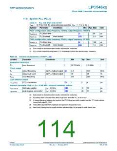
11.6 System PLL (PLL0)
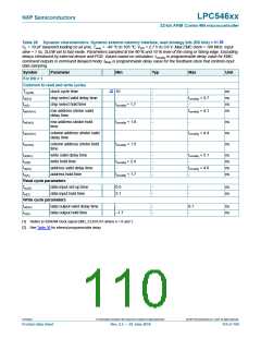
Table 31. PLL lock times and current
amb = 40 C to +105 C, unless otherwise specified. VDD = 1.71 V to 3.6 V
T
Symbol Parameter Conditions Min Typ Max
Unit
PLL0 configuration: input frequency 12 MHz; output frequency 100 MHz
[1]
tlock(PLL0)
IDD(PLL0)
PLL0 lock time
PLL0 current
96
s
[1][2]
when locked
-
-
2.0
mA
PLL0 configuration: input frequency 32 kHz; output frequency 100 MHz
[1]
tlock(PLL0)
IDD(PLL0)
PLL0 lock time
PLL0 current
-
-
-
-
108
1.6
s
[1][2]
when locked
mA
[1] Data based on characterization results, not tested in production.
[2] PLL current measured using lowest CCO frequency to obtain the desired output frequency.
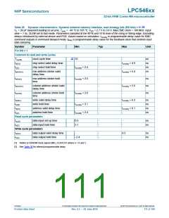
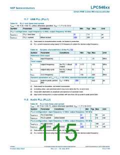
Table 32. Dynamic characteristics of the PLL0[1]
Symbol
Parameter
Conditions
Min
Typ Max
Unit
Reference clock input
Fin
input frequency
32.768 kHz -
25 MHz
Clock output
[2]
[3]
fo
output frequency
output duty cycle
CCO frequency
for PLL0 clkout output
for PLL0 clkout output
4.3
46
-
-
-
550
54
MHz
%
do
fCCO
275
550
MHz
Lock detector output
lock(PFD) PFD lock criterion
1
2
4
ns
Dynamic parameters at fout = fCCO = 540 MHz; standard bandwidth settings
[4][5]
Jrms-interval
Jpp-period
RMS interval jitter
fref = 10 MHz
fref = 10 MHz
-
-
15
40
30
80
ps
ps
[4][5]
peak-to-peak, period jitter
[1] Data based on characterization results, not tested in production.
[2] Excluding under- and overshoot which may occur when the PLL is not in lock.
[3] A phase difference between the inputs of the PFD (clkref and clkfb) smaller than the PFD lock criterion
means lock output is HIGH.
[4] Actual jitter dependent on amplitude and spectrum of substrate noise.
[5] Input clock coming from a crystal oscillator with less than 250 ps peak-to-peak period jitter.
LPC546xx
All information provided in this document is subject to legal disclaimers.
© NXP Semiconductors N.V. 2018. All rights reserved.
Product data sheet
Rev. 2.5 — 20 June 2018
114 of 169

 NXP [ NXP ]