Nano100(A)
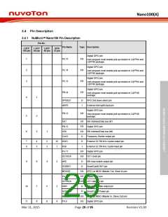
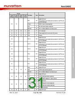
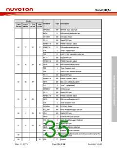
Pin No.
Pin Name
Type Description
LQFP
LQFP
LQFP
QFN
100-pin 64-pin
48-pin
33-pin
Digital GPIO pin
PB.7
I/O
User program must enable pull-up resistor in LQFP64 and
LQFP48 package.
22
13
CTSn1
nCS
I
O
I/O
P
UART1 Clear to Send input pin
EBI chip select enable output pin
SPI2 1st MOSI (Master Out, Slave In) pin
LDO output pin
MOSI20
LDO
23
24
25
14
15
16
10
11
12
6
7
8
VDD
P
Power supply for I/O ports and LDO source
Ground
VSS
P
Digital GPIO pin
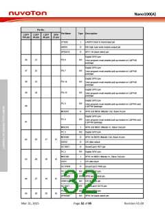
26
27
28
29
30
31
PE.12
PE.11
PE.10
PE.9
I/O
I/O
I/O
I/O
I/O
I/O
User program must enable pull-up resistor in LQFP64 and
LQFP48 package.
Digital GPIO pin
User program must enable pull-up resistor in LQFP64 and
LQFP48 package.
Digital GPIO pin
User program must enable pull-up resistor in LQFP64 and
LQFP48 package.
Digital GPIO pin
User program must enable pull-up resistor in LQFP64 and
LQFP48 package.
Digital GPIO pin
PE.8
User program must enable pull-up resistor in LQFP64 and
LQFP48 package.
Digital GPIO pin
PE.7
User program must enable pull-up resistor in LQFP64 and
LQFP48 package.
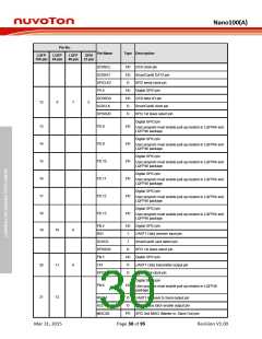
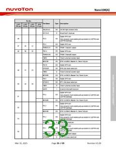
PB.0
I/O
I
Digital GPIO pin
32
33
17
18
13
14
9
RX0
UART0 Data receiver input pin
SPI1 1st MOSI (Master Out, Slave In) pin
Digital GPIO pin
MOSI10
PB.1
I/O
I/O
O
10
TX0
UART0 Data transmitter output pin
SPI1 1st MISO (Master In, Slave Out) pin
Digital GPIO pin
MISO10
PB.2
I/O
I/O
O
RTSn0
nWRL
SPICLK1
PB.3
UART0 Request to Send output pin
EBI low byte write enable output pin
SPI1 serial clock pin
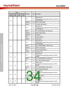
34
35
19
20
15
16
11
12
O
O
I/O
Digital GPIO pin
Mar 31, 2015
Page 31 of 95
Revision V1.00

 NUVOTON [ NUVOTON ]