M28R400CT, M28R400CB
SUMMARY DESCRIPTION
The M28R400C is a 4 Mbit (256Kbit x 16) non-vol-
atile Flash memory that can be erased electrically
at the block level and programmed in-system on a
Word-by-Word basis. These operations can be
performed using a single low voltage (1.65 to
2.2V) supply. VDDQ allows to drive the I/O pin
down to 1.65V. An optional 12V VPP power supply
is provided to speed up customer programming.
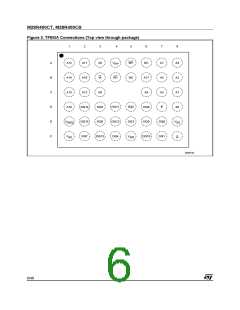
The memory is offered in a TFBGA46 (0.75mm
pitch) package and is supplied with all the bits
erased (set to ’1’).
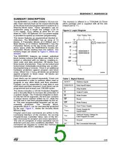
Figure 2. Logic Diagram
V
V
V
DD DDQ PP
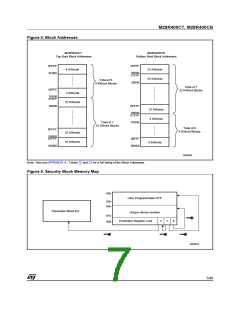
The device features an asymmetrical blocked ar-
chitecture. The M28R400C has an array of 15
blocks: 8 Parameter Blocks of 4 KWord and 7
Main Blocks of 32 KWord. M28R400CT has the
Parameter Blocks at the top of the memory ad-
dress space while the M28R400CB locates the
Parameter Blocks starting from the bottom. The
memory maps are shown in Figure 4., Block Ad-
dresses.
18
16
A0-A17
DQ0-DQ15
W
E
M28R400CT
M28R400CB
G
The M28R400C features an instant, individual
block locking scheme that allows any block to be
locked or unlocked with no latency, enabling in-
stant code and data protection. All blocks have
three levels of protection. They can be locked and
locked-down individually preventing any acciden-
tal programming or erasure. There is an additional
hardware protection against program and block
erase. When VPP ≤ VPPLK all blocks are protected
against program or block erase. All blocks are
locked at power-up.
RP
WP
V
SS
AI04392
Each block can be erased separately. Erase can
be suspended in order to perform either read or
program in any other block and then resumed.
Program can be suspended to read data in any
other block and then resumed. Each block can be
programmed and erased over 100,000 cycles.
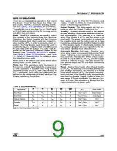
Table 1. Signal Names
A0-A17
Address Inputs
DQ0-DQ15
Data Input/Output
Chip Enable
E
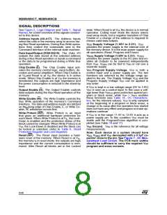
The device includes a 128 bit Protection Register
and a Security Block to increase the protection of
a system design. The Protection Register is divid-
ed into two 64 bit segments, the first one contains
a unique device number written by ST, while the
second one is one-time-programmable by the us-
er. The user programmable segment can be per-
manently protected. The Security Block,
parameter block 0, can be permanently protected
by the user. Figure 5., shows the Security Block
Memory Map.
G
Output Enable
Write Enable
Reset
W
RP
WP
Write Protect
Core Power Supply
V
DD
Power Supply for
Input/Output
V
DDQ
Program and Erase commands are written to the
Command Interface of the memory. An on-chip
Program/Erase Controller takes care of the tim-
ings necessary for program and erase operations.
The end of a program or erase operation can be
detected and any error conditions identified. The
command set required to control the memory is
consistent with JEDEC standards.
Optional Supply Voltage for
Fast Program & Erase
V
V
PP
SS
Ground
NC
Not Connected Internally
5/48

 NUMONYX [ NUMONYX B.V ]